What is Atomic Force Microscopy (AFM)
Atomic Force Microscopy (AFM) is a high-resolution non-optical imaging technique first demonstrated by Binnig, Quate and Gerber in 1985 [1]. Since then it has developed into a powerful measurement tool for surface analysis. AFM allows accurate and non-destructive measurements of the topographical, electrical, magnetic, chemical, optical, mechanical, etc. properties of a sample surface with very high resolution [2] in air, liquids or ultrahigh vacuum. This unique combination of capabilities makes AFM indispensable in most advanced science and technology labs around the world.
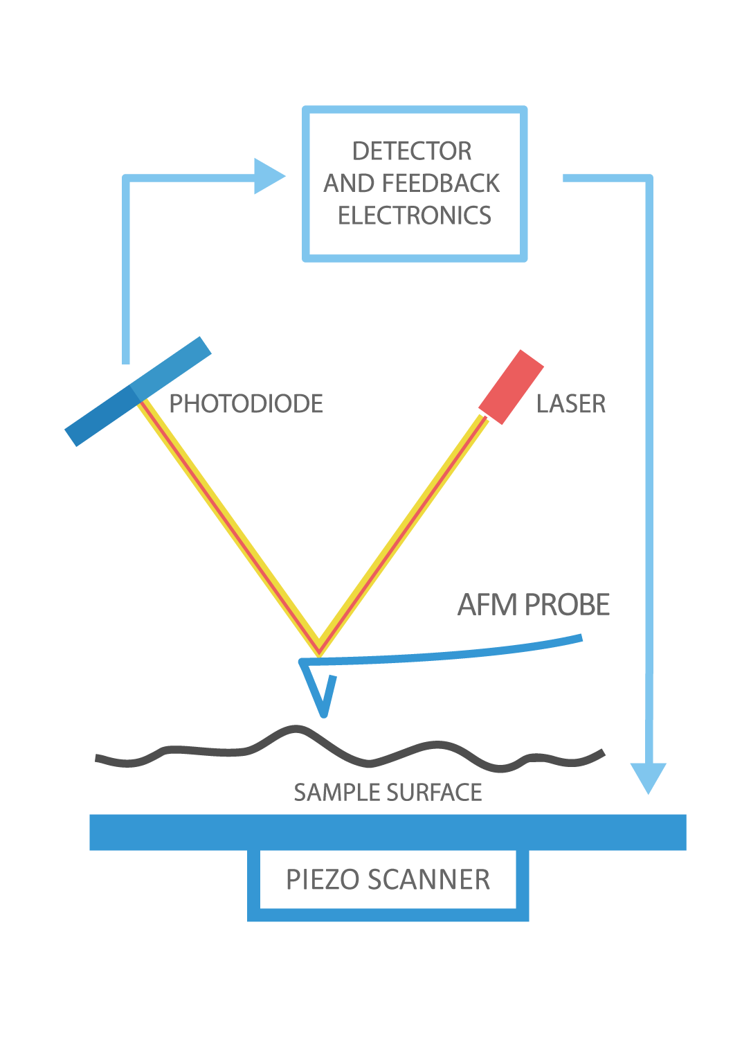
The basic operation principle of a standard AFM system with optical feedback [3] (Fig.1) involves scanning an AFM probe with a sharp AFM tip over a sample surface in a raster pattern. The AFM tip is usually made of silicon or silicon nitride and is integrated near the free end of a flexible AFM cantilever. A piezoelectric ceramic scanner controls the lateral and the vertical position of the AFM probe relative to the surface. As the AFM tip moves over features of different height the deflection of the AFM cantilever changes. This deflection is tracked by a laser beam reflected from the back side of the AFM cantilever and directed into a position sensitive photodetector. A feedback loop controls the vertical extension of the scanner in order to maintain near-constant AFM cantilever deflection and hence a constant interaction force. The coordinates that the AFM tip tracks during the scan are combined to generate a three-dimensional topographic image of the surface.
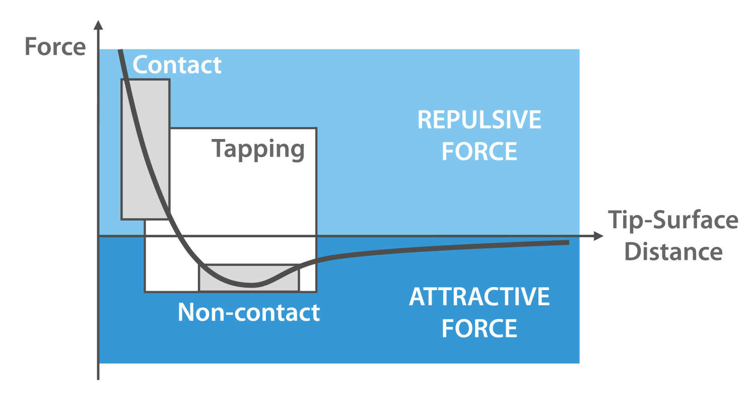
There are two basic modes of imaging surface topography with an Atomic Force Microscope: Static or Contact Mode and Dynamic Mode. Dynamic Mode is further sub-divided into Tapping or Intermittent Contact and Non-Contact Mode depending on the interaction forces between the AFM tip and the surface.
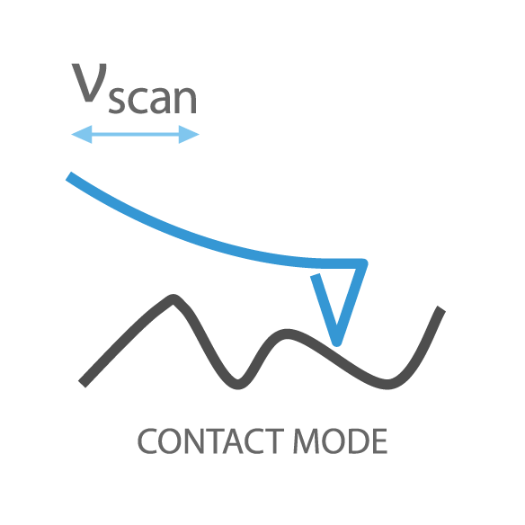
1. In Contact Mode, the AFM probe tip is scanned across the sample surface while maintaining constant contact with it (Fig.2). The feedback system aims to maintain constant AFM cantilever deflection and consequently a constant interaction force. The forces between the AFM tip and the surface are repulsive (Fig. 3). Soft AFM cantilevers with force constants ≤1N/m are usually used in order to minimize AFM tip wear and surface damage and in order to increase sensitivity.
Among the main drawbacks of Contact Mode operation are the susceptibility of AFM tips on soft AFM cantilevers to both lateral forces and sticking to the surface contamination layer that is present on most surfaces in ambient air. These result in image distortions. In addition, lateral forces can be damaging to the AFM probe tip and to soft samples.
Browse AFM probes for contact mode with C<1N/m
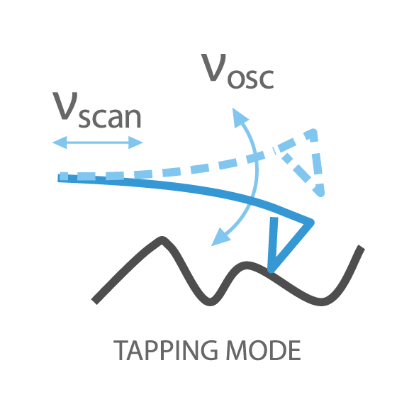
2. In Tapping Mode, the AFM probe cantilever is oscillated by a piezoelectric actuator at or near its fundamental resonance frequency, usually several tens to several hundred kilohertz. The AFM probe is lowered towards the sample surface so that the AFM probe tip slightly touches the surface at the lower end of the AFM cantilever oscillation (Fig. 4) and its oscillation amplitude is damped. The feedback loop maintains a constant AFM cantilever oscillation amplitude and hence a constant interaction force. The forces that dominate the interaction between the AFM tip and the surface are repulsive (Fig. 3).
Stiff AFM cantilevers with force constants in the range of 10-100N/m and high resonance frequencies >190kHz are used for standard Tapping Mode operation. These AFM cantilevers do not suffer from sticking to the surface when measuring in ambient air. For measuring soft samples, e.g. living cells, softer AFM cantilevers with force constants <10N/m and sometimes as low as sub-0.1N/m are used.
Browse AFM probes for standard tapping mode with C>10N/m and f≥190kHz
Browse AFM probes for soft tapping mode with C<10N/m and f<190kHz
3. In Non-Contact Mode the AFM cantilever is oscillated at or near its resonance frequency with a smaller amplitude (1nm or less) than in Tapping Mode and the AFM probe tip is kept at a distance of several nanometers to several tens of nanometers away from the surface (Fig. 5) in the region of attractive interaction forces [4] (Fig. 3). In some cases, the feedback loop maintains a constant AFM cantilever oscillation frequency and hence a constant interaction force (FM-AFM). This method gives more precise force control and super high-resolution images in liquid.
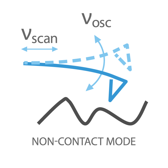
The advantage of Non-Contact Mode is that it offers the lowest possible interaction between the tip and the sample surface. Small interaction forces help preserve AFM tip sharpness and achieve high resolution. The disadvantage is that it is challenging to keep at the AFM tip in the attractive regime. For small tip-surface distances, high performance feedback controls are needed.
AFM cantilevers with high force constants and high resonance frequencies are most suitable for Non-Contact Mode.
Browse AFM probes for non-contact mode with C>25N/m and f≥190kHz
Beside topography, Atomic Force Microscopy allows investigating a variety of other surface properties. These additional imaging techniques are based on one of the three basic modes of operation. They help extract additional information about the sample surface simultaneously with its topography.
Some of these modes such as e.g. EFM and MFM often use the secondary technique Two-Pass Mode a.k.a. Lift Mode or Hover Mode. In Lift Mode the AFM acquires topography data and electric or magnetic data on the same scan line independently. The first pass is a regular topographic scan. During the second pass, second line scan or retrace scan, the AFM tip traces the surface topography at a preset vertical distance, usually 5-50nm, gathering information about the long-range electrostatic, magnetic, etc. forces via changes in the resonance frequency or phase of the AFM cantilever oscillation.
More recently developed Single-Pass Methods allow gathering topographic and other data simultaneously in a single pass with the help of lock-in amplifiers with improved sensitivity and higher resolution.
Below is a list of some commonly used additional imaging techniques.
1. Phase Imaging: Recording the phase difference between the drive signal and the AFM cantilever oscillation in dynamic mode gives additional information about material properties such as elasticity, adhesion, etc.
Browse AFM probes for phase imaging of hard materials with C>25N/m
Browse AFM probes for phase imaging of soft materials with C<25N/m
2. AFM in Liquids: Measurements of biological and other samples in aqueous solutions are possible in both Contact and Tapping Mode. For applications in liquids, silicon nitride probes are commonly used. Measuring with soft AFM cantilevers in liquids helps avoid sample surface damage by the AFM tip.
Browse AFM probes for tapping mode in fluids with gold coating and f>50kHz
Browse all AFM probes for various modes of AFM in liquids with gold coating
3. High-Speed Scanning (HSS): By increasing the scanning speed and the feedback speed up to video rates with the help of AFM cantilevers with megahertz resonance frequencies and high-speed electronics, dynamic processes in bioresearch can be visualized.
Browse high speed scanning AFM probes with f>300kHz
4. Ultrahigh Vacuum (UHV) AFM: AFM measurements under UHV allow performing atomic resolution imaging by protecting the sample surface from water film formation and contamination.
Browse AFM probes for vacuum AFM with high Q-factor
5. Force Modulation (FM) Microscopy: While scanning in Contact Mode, a periodic signal mechanically drives the AFM cantilever in the vertical direction [5]. The amplitude of AFM cantilever modulation varies according to the elastic properties of the sample which allows to map the sample’s elastic response.
Browse force modulation AFM probes, usually with C=2-3N/m and f=60-90kHz
6. Lateral Force Microscopy (LFM): By using a four-segment photodetector and scanning in Contact Mode, the microscope is capable of detecting not only the vertical deflection of the AFM cantilever but also its torsional twisting due to lateral forces (usually friction) acting on the AFM probe tip.
Browse AFM probes for lateral force microscopy with C<0.5N/m and torsional force constant Ctor<15N/m
7. Electrostatic Force Microscopy (EFM): The variations of the electric field gradient across the sample surface can be analyzed in Non-Contact Mode by applying a voltage bias to intermediately stiff AFM probes with an electrically conductive coating.
8. Kelvin Probe Force Microscopy (KPFM): Contact potential or work function mapping is possible by applying a DC and/or AC voltage bias.
9. Scanning Capacitance Microscopy (SCM): Local capacitance measurements are performed with electrically conductive AFM probes and high-frequency resonant-capacitance sensors, usually in order to determine carrier concentration in semiconductors. The technique is derived from Contact Mode and measures the changes in capacitance between the AFM tip and the sample surface while applying a combination of a DC and a high frequency AC voltage bias.10. Piezoresponse Force Microscopy (PFM): This mode exploits the reverse piezoelectric effect to investigate piezoelectric and ferroelectric materials by scanning a conductive AFM tip in Contact Mode and simultaneously applying an alternating voltage bias to induce mechanical deformation from the surface domains.
11. Conductive Atomic Force Microscopy (C-AFM): The local electrical resistivity of a surface can be measured with electrically conductive AFM probes in Contact Mode. A voltage difference is applied between the AFM probe and the sample the resulting electrical current is recorded. Scanning Spreading Resistance Microscopy (SSRM) is a closely related technique that scans a cross-sectional device area for determining dopant concentrations in semiconductors. Both techniques are very demanding on the AFM tip and require AFM probes with highly wear-resistant electrically conductive coatings. I-V Spectroscopy allows examining the bias dependent resistivity by ramping the voltage bias in Point-Contact Mode over a sample location of interest.
12. Magnetic Force Microscopy (MFM): AFM probes with a hard magnetic coating are used to investigate the magnetic field above a sample surface in Non-Contact Mode.
13. Force-distance (F vs d) Measurements: In this technique the AFM cantilever deflection is monitored as a function of piezo-displacement as the AFM probe tip approaches the sample, presses against it and then retracts from the surface. The obtained force-distance curve yields information about the stiffness and elasticity of the material at the point of contact, van der Waal’s forces, AFM tip adhesion forces, stretching forces of molecules, etc.
In Nanoindentation the approach curve is analyzed and in Adhesion Testing - the retract curve. Another related technique, Force Volume Mode takes a force-distance measurement at a predefined set of measurement point during a scan. AFM cantilevers with different stiffness can be used depending on the stiffness of the sample and the tradeoff between higher force sensitivity and higher maximum force.
Browse soft force-distance measurement AFM probes for bio and soft polymer samples with C<1N/m
Browse nanoindentation AFM probes with wear-resistant diamond or diamond-like carbon coating
Browse sphere nanoindentation AFM probes with well-defined sphere geometry
14.Pulsed Force Mode (PFM): By introducing an oscillation at a much lower frequency than the resonance frequency of the AFM cantilever, force-distance curves are taken at every point of an intermittent contact scan, thus mapping sample adhesion and stiffness.
A related technique, Chemical Force Microscopy (CFM) uses a chemically modified AFM tip to track the distribution of different chemical groups on the sample surface.
Browse soft pulsed force mode AFM probes for bio and soft polymer samples with C<1N/m
Browse stiff pulsed force mode AFM probes for hard samples
Browse sphere nanoindentation AFM probes with well-defined sphere geometry
15. ScanAsyst®**: Automated image optimization technology based on PeakForce Tapping™** and used in some Bruker AFM systems allows obtaining good quality AFM images as a turnkey solution regardless of the operator’s experience level.
Browse ScanAsyst®** compatible AFM probes
16. Nanolithography: Modifications of the sample surface can be obtained by applying sufficiently strong forces with the AFM probe tip (Scratch Lithography), by local oxidation of specific substrates such as titanium or silicon or by etching. The AFM tip can be moved across the sample surface along a predefined path to create structures with various shapes.
Browse nanolithography AFM probes with wear-resistant diamond or diamond-like carbon coating
17. Contact Resonance Microscopy: By measuring the resonance frequency of an AFM probe scanning a sample surface in Contact Mode while the sample is being shaken by a piezo actuator, the local elasticity of the material can be probed. AFM probes with various stiffness are used depending on the hardness of the sample
Browse contact resonance AFM probes, usually with C=2-3N/m for samples with M=1-10GPa or with C~15N/m for samples with M=10-50GPa
Browse contact resonance AFM probes with C>40N/m for samples with M>50GPa
18. Scanning Thermal Microscopy (SThM): Temperature and thermal conductivity measurements are possible when an AFM probe with a temperature sensor such as a thermocouple or a resistance thermometer is used.
Scanning thermal microscopy AFM probe with an integrated thin-film metal wire
19. Near-Field Scanning Optical Microscopy (NSOM, SNOM): Imaging with visible light with resolution beyond the diffraction limit is achieved the help of light-guiding AFM probes. NSOM is carried out either in aperture mode with a metal-coated AFM tip or in apertureless mode with a sharp uncoated AFM tip a.k.a. Scattering-Type SNOM (s-SNOM).
20. Tip-Enhanced Raman Spectroscopy (TERS) or Nano-Raman Spectroscopy: This technique allows chemical imaging beyond the diffraction limit. The Raman effect is used to provide chemical material identification by using monochromatic light and gathering backscattered light using the metal coated AFM tip as a nanometric near-field antenna.
21. AFM (Photothermal) Infrared Nanospectroscopy (AFM-IR): Infrared light absorption is detected by AFM via the thermal expansion of the sample near the AFM tip apex.
22. Electrochemical AFM (EC-AFM): This mode combines AFM with electrochemical measurements. Electrochemical reactions at a solid-liquid interface (conductive surface submerged in electrolyte) can be monitored in-situ by using an AFM tip with a metal wire as either the passive or the active electrode in a three-electrode electrochemical cell.
23. Scanning Tunneling Microscopy (STM): An electrically biased conductive AFM tip is scanned across a conductive sample surface at a sub-nanometer height. The topography is tracked by monitoring the tunneling current between the AFM tip and the sample. Either the Z-feedback is switched off and the tunneling current as a function of the lateral position is recorder (constant height mode) or the Z-feedback is on and a constant current is maintained (constant current mode). STM achieves extremely high resolution- 0.1nm laterally and 0.01nm vertically.
Strictly speaking, STM is not an AFM technique because of the different AFM probe and feedback setup. STM and AFM both comprise a class of techniques called Scanning Probe Microscopy (SPM). Nevertheless, STM deserves an honorable mention, because this technique, developed by Gerd Binnig and Heinrich Rohrer in 1981, is the direct predecessor of AFM.
This list is not exhaustive. There are many more AFM-based techniques such as:
Torsional Resonance Mode
Scanning Microwave Impedance Microscopy (SMIM)
Scanning Electrochemical Potential Microscopy (SECPM)
Critical Dimension AFM (CD-AFM)
Tunneling Current AFM (TUNA)
Atomic Force Profiling (AFP)
Photoconductive AFM (pcAFM)
PeakForce Tapping™**
PeakForce TUNA
PeakForce Quantitative Nanomechanical Property Mapping
Three-Dimensional Sidewall Imaging (3D-AFM)
Deep Trench AFM
Scanning Ion Conductance Microscopy (SICM)
etc.
The higher the resolution of an AFM image, the more information can be extracted about the smallest features on the sample surface.
The vertical (Z-axis) imaging resolution is probe-independent. On the other hand, the achieved lateral resolution is usually limited by the AFM probe tip geometry rather than by the capabilities of the microscope. A medium-level AFM is often capable of achieving sub-nanometer lateral resolution and sub-Angstrom vertical resolution. The high-quality standard AFM probes offered by NanoAndMore have sub-10nm AFM tip radii and allow low nanometer resolution. High-resolution AFM probes with AFM tip radii in the range 1-5nm enable atomic or near-atomic resolution on atomically flat surfaces. Naturally, high resolution can be achieved only if the original extreme sharpness of the AFM tip is preserved during the measurement by scanning in optimal conditions that limit AFM tip wear and AFM tip contamination.
Browse supersharp AFM probes with 1-5nm AFM tip radius