

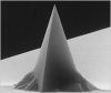
Happy Swiss National Holiday with Smallest Swiss CrossWed Jul 31 2019


Ferroelectricity-free lead halide perovskites – NANOSENSORS™Sun Jul 21 2019
Highlights


AFM Probe Focus


best of the best
qp-HBC
uniqprobe™ - HeartBeat Cantilever for ScanAsyst®** and Peak Force Tapping™**
Coating:
Reflective Aluminum
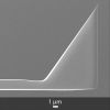
Tip Shape: Circular symmetric
Tip Shape: Circular symmetric
AFM Cantilever:
F
60 kHz
C
0.5 N/m
L
115 µm
ATEC-NC
Tapping Mode AFM Probe with REAL Tip Visibility
Coating:
none
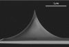
Tip Shape: Visible
Tip Shape: Visible
AFM Cantilever:
F
335 kHz
C
45 N/m
L
160 µm
TESPA
Standard Tapping Mode AFM Probe
Coating:
Reflective Aluminum
Tip Shape: Standard
Tip Shape: Standard
AFM Cantilever:
F
320 kHz
C
42 N/m
L
125 µm
OTESPA
Standard Tapping Mode AFM Probe with AFM Tip at the Very End of the AFM Cantilever
Coating:
Reflective Aluminum
Tip Shape: Optimized Positioning
Tip Shape: Optimized Positioning
AFM Cantilever:
F
300 kHz
C
26 N/m
L
160 µm