This note is a brief guide to silicon AFM probe fabrication. It is intended for those who want to learn about how AFM probes are produced and have little or no experience in the field of semiconductor technology.
Silicon AFM probes are fabricated on single crystal silicon wafers. The wafers are patterned in a micromachining process in order to obtain the desired structures. The general step sequence for one structuring step is shown below. The outline of the process is the following: a photosensitive film (photoresist) is deposited on the wafer surface. This film is structured by selectively exposing only certain parts of it to light through a patterned photomask and developing it. Then the structures are transferred to the silicon substrate or the layer beneath the photoresist by etching (dissolving) it in a chemically reactive solution.
The exposition (step 4) is done through a mask with a repeatable pattern which allows transferring simultaneously a big number of identical structures on to the wafer. This makes the process much more efficient than single unit production. Usually, several hundred AFM probes are produced from one silicon wafer.
Various cleaning steps are performed at different stages of processing. They are of immense importance to the fabrication process. Cleaning removes residual particles and chemicals from the wafer surface thus significantly decreasing defect density and greatly improving yield.
‘Yield’ is a very important word in the world of microfabrication. In order to achieve high overall yields, the yields of individual steps must be orders of magnitude higher. Therefore, every single processing step must be carried out with great care and under strict control over process parameters.
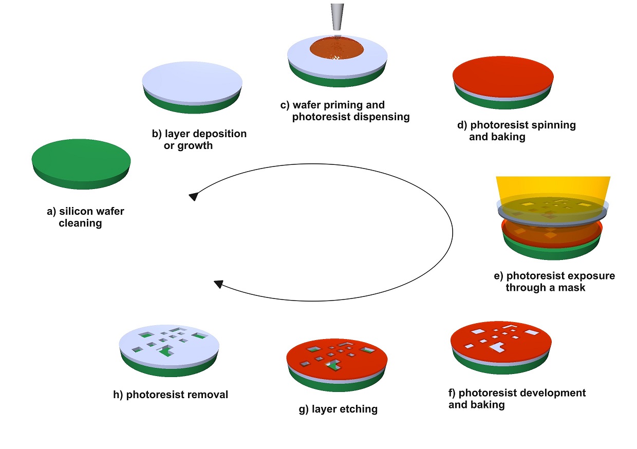
The AFM probe fabrication process usually consists of more than 100 steps and it takes a couple of months to complete. The process flow described below is a simplified version of an actual fabrication process.
Three photolithography steps are needed for producing a silicon AFM probe: one for the chip, a second for the AFM cantilever and a third for the AFM tip.
Some simplifications are made in order to keep the overview more concise and clearer. The photoresist deposition, exposition, development and removal steps are combined in ‘photolithography’ steps and the cleaning steps are omitted.


The finished silicon wafer contains several hundred AFM probes. The AFM probes are attached to the wafer only by two small silicon bridges on each side of the holder chip. The AFM probes can be easily freed by applying a small mechanical force to the holder chip with tweezers.


The actual fabrication process varies for different AFM probe types and for different manufacturers. Different technological processes, process parameters and step sequences are applied. This has a significant impact on the final product quality and yield. At the end, it is up to the customers to find the right AFM probes that satisfy their requirements.