Latest News

nanotools Coating that Mimics Topography and Perspiration Behavior of Human Fingertips - news

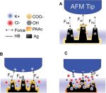
Coating that Mimics Topography and Perspiration Behavior of Human FingertipsWed Nov 27 2024

Discover how nanotools biosphere™ with 20nm radius are applied to recording force maps in contact mode and then extract the Young’s modulus in different areas of the coating.
  • Title: Reversible Perspiring Artificial “Fingertips”
    DOI: https://doi.org/10.1002/adma.202209729
  • Authors: Dongyu Zhang, Jacques Peixoto, Yuanyuan Zhan, Mert O. Astam, Tom Bus, Joost J. B. van der Tol, Dirk J. Broer, Danqing Liu
  • Publication: Advanced Materials
  • Publisher: Wiley-VCH GmbH
  • Date: 06 February 2023

NanoWorld Local probing of the nanoscale hydration landscape of kaolinite basal facets in the presence of ions - news

Local probing of the nanoscale hydration landscape of kaolinite basal facets in the presence of ionsTue Nov 26 2024

Kaolinite is one of the most abundant natural clay minerals within soils at the Earth's surface and within rock units in the upper crust. *
The interface between aqueous solutions and the facets of kaolinite plays an important role in a wide range of technological applications including #tribology, paper production, oil recovery, waste water treatment and medical devices. *
This is made possible by kaolinite's layered structure, with its two basal surfaces -#aluminol and #siloxane-exhibiting different properties and reactivity. *
Both macroscopic and #nanoscale studies point to a strong dependence of kaolinite's surface properties on its local hydration structure. No experimental results, however, have systematically and comparatively investigated the hydration landscape of both basal facets to date. *
In the article “Local probing of the nanoscale hydration landscape of kaolinite basal facets in the presence of ions” Clodomiro Cafolla, Tai Bui, Tran Thi Bao Le, Andrea Zen, Weparn J. Tay, Alberto Striolo, Angelos Michaelides, Hugh Christopher Greenwell and Kislon Voïtchovsky combine high-resolution #atomicforcemicroscopy ( #AFM) imaging and #forcespectroscopy with classical molecular dynamics (MD) simulations to illustrate key differences in the hydration behaviour of the aluminol and siloxane facets of kaolinite particles immersed in water and NaCl solutions. *
This combined approach allows the authors to overcome the limitations of each technique via the advantages of the other. Specifically, AFM images highlight the differences in the first hydration layer of each facet and serve as a basis for force spectroscopy measurements of the full hydration profile at a given location. *
Water densities extracted from MD help interpret the AFM results, both in the absence and in the presence of added Na+ ions. *
Complementary #AFMspectroscopy measurements show an excellent agreement between the conservative component and MD's water density profiles, with discrete hydration layers on both facets and little sensitivity to added ions. *
The dissipative component of the measured AFM tip-sample interactions is more sensitive to the presence of ions, with MD suggesting a link with the local water dynamics and transient instabilities between stable hydration layers. *
These effects are facet-dependant and more pronounced on the aluminol facet where the first water layer is better defined. Increasing the salt concentration allows hydrated ions to form more stable layers, with hints of organised ionic domains. *
The results provide unique insights into both the equilibrium molecular structure and dynamics of the kaolinite facets, potentially informing applications involving interfacial processes. *
The AFM experiments were conducted at 25 ± 0.1 °C using a commercial #atomicforcemicroscope equipped with temperature control.
NanoWorld Arrow-UHF silicon #AFMprobes were used.
The #AFMcantilevers were thoroughly washed with pure water (20 times with 100 μl) and then with the solution of interest (40 times with 100 μl).
Experiments were performed at near neutral pH 5.8. This ensured that only the metal ions of interest were present on the AFM cantilever. Thorough cleaning procedures were implemented to avoid any possible sources of contamination. *
During the measurements, the AFM cantilever and the sample were fully immersed in the aqueous ionic solution of interest. The thermal spectrum of the AFM cantilever was used to perform the flexural calibration of the AFM cantilevers. The AFM probes were found to have a flexural spring constant in the range 1.0–4.0 N/m and a resonance frequency of ∼400–900 kHz in water. These values agree with the nominal range and the literature. The AFM cantilever oscillation was photo-thermally driven to ensure greater stability, making sure that the frequency response remained unaffected by any spurious contributions due to the noise produced by mechanical coupling with other experimental components of the system. *
Please have a look at the NanoWorld blog for the full citation and a direct link to the full article:

MikroMasch MikroMasch® HQ:NSC35/Cr-Au AFM probes are used for phase composition-contrast measurements

MikroMasch® HQ:NSC35/Cr-Au AFM probes are used for phase composition-contrast measurementsMon Nov 18 2024

This study investigates the effects of water released from boehmite nanoparticles in polymer nanocomposites. While the incorporation of the nanoparticles in the epoxy increases its overall stiffness, water released from undried nanoparticles leads to the formation of a soft interface around them and a significant decrease in the crosslink density.
MikroMasch® HQ:NSC35/Cr-Au AFM probes are used for phase composition-contrast measurements.

NANOSENSORS A comparative nanotribological investigation on amorphous and polycrystalline forms of MoS2 - news

A comparative nanotribological investigation on amorphous and polycrystalline forms of MoS2Fri Nov 15 2024

#Molybdenumdisulfide ( #MoS2) is commonly used as a dry lubricant due to its enhanced performance in the absence of oxygen and its elevated temperature stability, which make it suitable for extreme environmental conditions. For these reasons, MoS2 has well-established applications in the automotive and aerospace industries, metal forming and cutting tools, electrical contacts, and nano- and micro-electromechanical systems.*
In this context, it is well-known that crystalline forms of MoS2 have better frictional properties as compared to amorphous ones. They are also less sensitive to humidity and atmospheric conditions.*
However, crystalline MoS2 tends to exfoliate during sliding if the loading forces are too high, resulting in high wear, coefficient of friction (COF), and low stability. To improve the design and durability of components based on MoS2 there is a need to explore the tribological behavior of MoS2 in alternative forms, and to characterize their early-stage #wearbehavior down to the #nanoscale.*
Experimental #characterizations such as those made possible by #atomicforcemicroscopy (AFM) are the most important tool to gain quantitative insights on the wear resistance of those #materials on the nanoscale.*
In the article “A comparative nanotribological investigation on amorphous and polycrystalline forms of MoS2” by Hesam Khaksar, Prashant Mittal, Nabil Daghbouj, Grzegorz Cios, Tomas Polcar and Enrico Gnecco, the wear behavior of two amorphous and polycrystalline forms of MoS2 prepared by magnetron sputtering is characterized in a combined nanoindentation and atomic force microscopy (#AFM) study supported by Raman and transmission electron microscopy (TEM) analysis.*
From the #morphology of wear tracks estimated after scratching the surfaces with a Berkovich indenter and a loading force up to 2 mN, the authors conclude that, on the microscale, both forms follow the Archard’s wear equation, and the wear resistance is about four times higher on the amorphous MoS2.*
The coefficient of #friction is much lower on the worn areas, which is associated to significant smoothing of the surfaces caused by the scratching process. With normal forces in the µN range, the analysis is made difficult by the fact that the linear dimensions of the wear tracks are comparable to those of the smallest surface features.
Even if the #Archardsequation looses validity, the #wearresistance is considerably larger on amorphous MoS2 also on the nanoscale.*
The results presented by Hesam Khaksar et al. conclude that the polycrystalline form of MoS2 has poor tribological properties at the micro/-nanoscale as compared to the amorphous form and hence less suited as a solid coating in ambient conditions.*
NANOSENSORS™ diamond coated PointProbe®Plus DT-NCHR AFM probes (typical force constant: 80 n/m, typical macroscopic AFM tip radius of curvature between 100 and 200 nm) were used to create the scratches and capture the images, allowing for a detailed examination of the surface features and material properties.
For AFM-based friction measurements, NANOSENSORS™ PointProbe®Plus PPP-LFMR AFM probes, with a typical force constant of 0.2 N/m were employed.
NANOSENSORS™ PointProbe®Plus PPP-NCHR AFM probes (typical force constant: 42 N/m typical resonance frequency 330 kHz) were used for standard tapping mode imaging.
Please have a look at NANOSENSORS blog for the full citation and a direct link to the full article: https://www.nanosensors.com/…/a-comparative…/

sQube sQube colloidal AFM probes with 3.3µm SiO2 microspheres on soft silicon nitride AFM cantilevers (0.08N/m) are used for accurate measurements of the interaction forces with graphene sheets deposited on silicon wafers. - news

sQube colloidal AFM probes with 3.3µm SiO2 microspheres on soft silicon nitride AFM cantilevers (0.08N/m) are used for accurate measurements of the interaction forces with graphene sheets deposited on silicon wafers.Fri Nov 15 2024

“Graphene-water interface is electrically charged. The broad evidence presented in this paper from a variety of different techniques shows that the favorable interaction between hydroxide ions and graphene is the reason for this charge, which allows the preparation of additives-free, stable aqueous graphene dispersions. A posteriori, this fact is not enigmatic, and indeed, it becomes flawless in hindsight: charged interfaces are the rule, and non-charged interfaces are clearly the exception.”
 

NanoAndMore University College Groningen Open Day

Seeing so much enthusiasm for science gives us great hope for the future!Tue Nov 12 2024

NanoAndMore Europe would like to thank the organizers and participants of the 2024 Dutch #ScanningProbeMicroscopy Day for the opportunity to attend. The event, hosted at the @universityofgroningen, was organized by Prof. Roberto Lo Conte , and the venue, the Feringa Building, was truly impressive with its fascinating architecture.
Alongside the high-calibre presentations, we enjoyed many engaging conversations at our booth. We were also delighted to meet numerous curious and bright students who, as part of the University College Groningen Open Day happening simultaneously, found their way to our booth.
Seeing so much enthusiasm for science gives us great hope for the future!

NanoAndMore NanoAndMore GmbH will have a booth that this year’s Dutch SPM Day on Friday, November 8th, 2024.

NanoAndMore GmbH will have a booth that this year’s Dutch SPM Day on Friday, November 8th, 2024.Fri Nov 08 2024

Meet us at Zernike Campus, at University of Groningen and find out more about the many #AFMprobes from well-known manufacturers such as NANOSENSORS NanoWorld , nanotools , BudgetSensors , MikroMasch , Opus, Olympus and sQube we offer and feel free to discuss your #atomicforcemicroscopy applications with us.
The Dutch Scanning Probe Microscopy Day is an annual one-day conference that aims at bringing together experts from all fields of #scanningprobemicroscopy research in academia as well as industry within the Netherlands, Belgium and Germany.
Invited speakers this year are:
- Pavel Jelinek (Czech Academy of Sciences) talking about:
Resolving anisotropic charge and spin on atomic scale using a functionalized SPM probe
- Alex Weber-Bargioni (Lawrence Berkeley National Laboratory), talking about:
Where does SPM fit into next generation quantum materials explorations
- Kirsten von Bergmann (University of Hamburg), talking about:
Complex magnetic order and interplay of magnetic films with superconductivity
We hope to see you in Groningen soon!

nanotools Next Generation Biomaterial for Advanced Delivery Systems for Immunotherapy - news

Next Generation Biomaterial for Advanced Delivery Systems for ImmunotherapyFri Oct 25 2024

Discover how nanotools MSS-soft 13deg with 2.8N/m cantilevers, 2nm radius and 15nm diameter measured at 150nm from apex are applied to study the nanoscale architectural features of Ca(OH)2-modified T. weissflogii.
  • Title: Modification of Living Diatom, Thalassiosira weissflogii, with a Calcium Precursor through a Calcium Uptake Mechanism: A Next Generation Biomaterial for Advanced Delivery Systems
    DOI: 10.1021/acsabm.4c00431
  • Authors: Isma Liza Mohd Isa, Akshay Srivastava, David Tiernan, Peter Owens, Peadar Rooney, Peter Dockery, and Abhay Pandit
  • Publication: ACS Applied Bio Materials
  • Publisher: American Chemical Society
  • Date: June 17, 2024

BudgetSensors 463867556_1066234268836217_7109228420922185010_n.jpg

Check out this investigation of the effects of contaminants in the liquid meniscus between the AFM tip and the sample on conductivity.Mon Oct 21 2024

Trying to make sense of your Conductive AFM and I-V spectroscopy measurements? Check out this investigation of the effects of contaminants in the liquid meniscus between the AFM tip and the sample on conductivity. ElectroCont-G and other AFM probes are used in the tests.

NanoAndMore NAMjp.jpg

@NanoAndMore Japan is exhibiting at the 10t International Symposium on Surface Science in Kita-kyushu, Fukuoka, Japan this weekMon Oct 21 2024

@NanoAndMore Japan https://www.nanoandmore.jp/ is exhibiting at the 10t International Symposium on Surface Science in Kita-kyushu, Fukuoka, Japan https://www.jvss.jp/conference/isss10/scope.html this week.
Please drop by our booth at the Kitakyushu International Conference Center to learn more about the many different #AFMprobe types from NanoWorld , NANOSENSORS , nanotools , BudgetSensors , MikroMasch , Olympus and sQube we offer and feel free to discuss your #atomicforcemicroscopy applications with us.

MikroMasch MMPost.jpg

Potential-dependent superlubricity of stainless steel and Au(111) using a water-in-surface-active ionic liquid mixtureTue Oct 15 2024

“Achieving and controlling superlubricity to enable energy conservation remains a substantial challenge, despite progress in the development of high-performance lubricants… For the first time, superlubricity has been observed in a water-in-SAIL mixture (1.6 M [BMIm][AOT]) at positively charged Au(1 1 1) and stainless steel. It results from the AFM tip sliding over fluid water molecules in the hydration layer of well-defined [AOT]− bilayers. Superlubricity persists up to a critical normal force, beyond which friction jumps to a high level.”
Friction and normal force AFM measurements have been carried out with HQ:NSC36 series AFM probes.

NanoWorld Real-time multistep asymmetrical disassembly of nucleosomes and chromatosomes visualized by high-speed atomic force microscopy - news

Real-time multistep asymmetrical disassembly of nucleosomes and chromatosomes visualized by high-speed atomic force microscopyThu Oct 03 2024

During replication, expression, and repair of the #eukaryoticgenome, cellular machinery must access the DNA wrapped around histone proteins forming nucleosomes. These octameric #proteinDNA complexes are modular, dynamic, and flexible and unwrap or disassemble either spontaneously or by the action of molecular motors. Thus, the mechanism of formation and regulation of subnucleosomal intermediates has gained attention genome-wide because it controls DNA accessibility.*
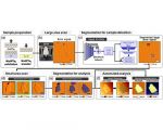
In the article “Real-Time Multistep Asymmetrical Disassembly of Nucleosomes and Chromatosomes Visualized by High-Speed Atomic Force Microscopy” Bibiana Onoa, César Díaz-Celis, Cristhian Cañari-Chumpitaz, Antony Lee and Carlos Bustamante describe how they imaged #nucleosomes and their more compacted structure with the linker histone H1 (#chromatosomes) using #highspeedatomicforcemicroscopy to visualize simultaneously the changes in the DNA and the histone core during their disassembly when deposited on mica.*
Furthermore, Bibiana Onoa et al. trained a neural network and developed an automatic algorithm to track molecular structural changes in real time. *
The authors’ results show that nucleosome disassembly is a sequential process involving asymmetrical stepwise dimer ejection events. The presence of H1 restricts DNA unwrapping, significantly increases the nucleosomal lifetime, and affects the pathway in which heterodimer asymmetrical dissociation occurs. *
Bibiana Onoa et al. observe that #tetrasomes are resilient to disassembly and that the tetramer core (H3·H4)2 can diffuse along the nucleosome positioning sequence. Tetrasome mobility might be critical to the proper assembly of nucleosomes and can be relevant during nucleosomal transcription, as tetrasomes survive RNA polymerase passage. These findings are relevant to understanding nucleosome intrinsic dynamics and their modification by DNA-processing enzymes. *
To characterize the nucleosomes dynamics in 2D, individual molecules were observed in buffer using an Ando-type high speed atomic force microscope together with NanoWorld Ultra-Short Cantilevers for HS-AFM of the USC-F1.2-K0.15 type (typical spring constant 0.15 N/m, typical resonance frequency in air 1200 kHz, resonance frequency 500–600 kHz in liquid). *
The AFM data presented in the article allow the authors to directly visualize the dynamics of DNA and histones during nucleosome and chromatosome disassembly, providing a simultaneous observation of DNA unwrapping and histone dissociation. *
The experimental and analytical strategy presented shows that real-time #HSAFM is a robust and powerful tool for studying #singlenucleosomes and #chromatindynamics. *
Please have a look at the NanoWorld blog for the full citation and a direct link to the full article

BudgetSensors Combined confocal microscopy and atomic force microscopy with BudgetSensors ElectriCont-G and MagneticMulti75-G AFM probes

Combined confocal microscopy and atomic force microscopy with our ElectriCont-G and MagneticMulti75-G AFM probes demonstrate sub-diffraction localization of luminescent defects and nitrogen vacancy center based magnetometry.Mon Sep 30 2024

"The setup demonstrates ≈10 nm resolution in PL imaging of shallow NV centers in diamond and shows the ability to separately address NV centers unresolvable with optical means. The results indicate that in contrast to gold cantilevers, platinum tips of the same diameter do not exhibit a significant plasmon-related PL enhancement, while still inducing a PL quenching at the lateral NV-tip distances comparable to the tip diameter. This nanoscale localization can be utilized to determine the position of single NV centers in diamond nanopillars with high precision, which is crucial for the scanning NV magnetometry."


NANOSENSORS Carbon Thin-Film Electrodes as High-Performing Substrates for Correlative Single Entity Electrochemistry - news

Carbon Thin-Film Electrodes as High-Performing Substrates for Correlative Single Entity ElectrochemistryThu Sep 26 2024

#Singleentityelectrochemistry (SEE) is an emerging area of research that aims at evaluating the electrochemical response of #materials at the micro- and #nanoscale. *
SEE in combination with complementary #characterization techniques has opened the door to a new type of characterization known as correlative-SEE that holds exceptional potential toward understanding #nanomaterials for energy applications. In such methods, spectroscopy and/or microscopy are used in tandem with SEE to correlate the electrochemical response to chemical and/or structural properties of probed entities. *
In the article “Carbon Thin-Film Electrodes as High-Performing Substrates for Correlative Single Entity Electrochemistry” Marc Brunet Cabré, Christian Schröder, Filippo Pota, Maida A. Costa de Oliveira, Hugo Nolan, Lua Henderson, Laurence Brazel, Dahnan Spurling, Valeria Nicolosi, Pietro Martinuz, Mariangela Longhi, Faidra Amargianou, Peer Bärmann, Tristan Petit, Kim McKelvey and Paula E. Colavita discuss properties and demonstrate applications of #graphitizedcarbonthinfilmelectrodes as substrates for correlative-SECCM.*
The authors first discuss chemical and structural properties of these films and how they can be tuned through synthesis/deposition conditions to deliver several of the above-mentioned requirements of correlative-SECCM. *
Marc Brunet Cabré et al. demonstrate the capability and versatility of these substrates using three nano-entities of very distinct morphological and chemical composition, such as #carbonencapsulatednickelnanoparticles ( Ni@C), #carbonnanocubes (CNC), and #2DMXenes (Ti3C2Tx). Correlative-SEE of these was achieved by coupling SECCM with a range of widely accessible scanning microscopies, including scanning electron microscopy (SEM), energy-dispersive spectroscopy (EDS), and #atomicforcemicroscopy ( #AFM). *
Finally, Marc Brunet Cabré et al. demonstrate correlative-SEE applications that integrate advanced synchrotron techniques such as scanning X-ray microscopy (SXM) in transmission and total electron yield (TEY) modes. Using SXM the authors show that it is possible to obtain both nm-resolution imaging and spectroscopic chemical information from X-ray absorption spectra (XAS) on these thin films substrates to correlate against the electrochemical response of nano-entities. *
@NANOSENSORS PointProbe® Plus PPP-NCHR #AFMprobes (typical resonance frequency: 330 kHz, typical force constant: 42 N/m) were used for the atomic force microscopy (AFM) characterization in non-contact mode.

NanoWorld Kinetic-controlled Crystallization of α-FAPbI3 Inducing Preferred Crystallographic Orientation Enhances Photovoltaic Performance - news

Kinetic-controlled Crystallization of α-FAPbI3 Inducing Preferred Crystallographic Orientation Enhances Photovoltaic PerformanceThu Sep 19 2024

Physical properties of #polycrystallinematerials are mostly determined by their #microstructure. As the #crystallizationprocess can determine the microstructure, the nucleation, and growth can also control whether the materials will be resulted in single crystalline or polycrystalline. Along with the morphological changes, anisotropic properties of the materials can also be controlled. *
As a result, #preferentialorientation with advanced optoelectronic properties can enhance the #photovoltaic devices' performance. *
Although incorporation of additives is one of the most studied methods to stabilize the photoactive α-phase of formamidinium lead tri-iodide (α-FAPbI3), no studies focus on how the additives affect the crystallization kinetics. *
In the article “Kinetic-Controlled Crystallization of α-FAPbI3 Inducing Preferred Crystallographic Orientation Enhances Photovoltaic Performance” along with the role of methylammonium chloride (MACl) as a “stabilizer” in the formation of α-FAPbI3, Sooeun Shin, Seongrok Seo, Seonghwa Jeong, Anir S. Sharbirin, Jeongyong Kim, Hyungju Ahn, Nam-Gyu Park and Hyunjung Shin point out the additional role as a “controller” in the crystallization kinetics. *
With microscopic observations, for example, electron backscatter diffraction and selected area electron diffraction, it is examined that higher concentration of MACl induces slower crystallization kinetics, resulting in larger grain size and [100] preferred orientation. *
Optoelectronic properties of [100] preferentially oriented grains with less non-radiative recombination, a longer lifetime of charge carriers, and lower photocurrent deviations in between each grain induce higher short-circuit current density (Jsc) and fill factor. *
Resulting MACl40 mol% attains the highest power conversion efficiency (PCE) of 24.1%.
The results provide observations of a direct correlation between the crystallographic orientation and device performance as it highlights the importance of crystallization kinetics resulting in desirable microstructures for device engineering. *
The #electricalcharacterizations with #atomicforcemicroscopy ( #AFM) and #conductiveatomicforcemicroscopy ( #CAFM) were done to measure the local conductance of FAPbI3 films. All measurements were performed under illumination (green LED) with a 1.3 V bias using a Pt-coated C-AFM probe (NanoWorld PlatinumIridium coated Pointprobe® CONTPt ). https://www.nanoworld.com/contact-mode-platinum-coated…
FTO was used for the conductive substrates.
Conductive atomic force microscopy (C-AFM) indicated much more homogeneous photocurrent generation along the surface of (100) preferentially oriented layers. *
Please have a look at the NanoWorld blog for the full citation and a direct link to the full article

NanoAndMore Japan Presents the Applied Physics Society Autumn Academic Lectures Annexhibition @JSAP NanoAndMore EXPO Autumn Exhibiting at 2024

今週、JSAP Expo Autum 2024 で NanoAndMore Japan にお越しくださいMon Sep 16 2024

NanoAndMoreジャパンは応用物理学会 秋季学術講演会 併設展示会 JSAP EXPO Autumn  - this is the main text
2024に出展しています。

 主催:公益社団法人 日本応用物理学会
 日時:2024年9月16日 (月)-9月20日(金)
 場所:新潟市 朱鷺メッセ ブーズ番号I-24

 https://meeting.jsap.or.jp/
 #AFMカンチレバー #AFMプローブ #日本応用物理学会 #応用物理学  #物理学 #SPMプローブ #原子間力顕微鏡 #走査型プローブ顕微鏡 #jsap #超高周波AFMプローブ #マイクロカンチレバー #ナノテクノロジー #材料科学 #生物物理学 #応用物理学 #走査型プローブ顕微鏡 学 #応用物理学 #走査型プローブ顕微鏡

NanoAndMore Japan Presents the Applied Physics Society Autumn Academic Lectures Annexhibition @JSAP NanoAndMore EXPO Autumn Exhibiting at 2024

Visit NanoAndMore Japan at JSAP Expo Autum 2024 this weekMon Sep 16 2024

NanoAndMore Japan is at 応用物理学会 JSAP EXPO Autumn exhibition held by the Japanese society for #appliedphysics this week. Please visit us at booth no. I-24 to learn all about the #AFMprobes we offer: NanoWorld , NANOSENSORS , Olympus , nanotools , BudgetSensors , MikroMasch and sQube #colloidalAFMprobes are all available from us.
   
   Organizer: The Japanese Society of Applied Physics (Japan)
   Date: Monday, September 16 - Friday, September 20, 2024
   Location: Niigata City Akagi Messe booth No. I-24


Loading
nanosensors-logo
nanoworld-logo
budgetsensors-logo
mikromasch-logo
opus-logo
sqube-logo
nanotools-logo