

Signal Origin of Electrochemical Strain Microscopy and Link to Local Chemical Distribution in Solid State Electrolytes via NANOSENSORS™Mon Apr 19 2021
Signal Origin of Electrochemical Strain Microscopy and Link to Local Chemical Distribution in Solid State Electrolytes
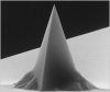
Solid state electrolytes (SSEs) are interesting materials that could potentially replace the currently used organic electrolytes in lithium‐ion batteries (LIBs). * Electrochemical strain microscopy (ESM), a research technique based on atomic force microscopy (AFM), was developed to locally probe ion movement in electrodes based on electro-chemo-mechanical coupling measure through the AFM cantilever deflection. It can […]
Want to find out which NANOSENSORS™ AFM probe was used for the research presented in this article or do you want the full citation and a direct link to the full research article? Then have a look at the NANOSENSORS™ blog to read more.

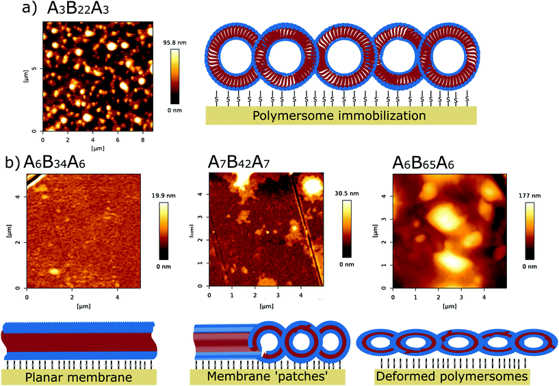
BudgetSensors® Tap150Al-G AFM probes used in a recent studyFri Apr 16 2021
Our Tap150Al-G AFM probes support the investigation of forming solid supported polymer membranes via vesicle fusion.


Van der Waals heterojunctions create new platform for photovoltaic and photodetector design via nanotoolsThu Apr 15 2021
Van der Waals heterojunctions create new platform for photovoltaic and photodetector design.


High-speed atomic force microscopy highlights new molecular mechanism of daptomycin action via NanoWorld®Wed Apr 14 2021
High-speed atomic force microscopy highlights new molecular mechanism of daptomycin action
The current pandemic is not the only health threat worldwide. Another worry is the increasing antibiotic resistance which increases the fear to run out of effective antibiotics. This is one of the reasons why antimicrobial peptides (AMPs) are gaining more and more interest. The lipopeptide Daptomycin ( DAP ) has been used as a …more


MikroMasch® AFM Probes in a recent studyTue Apr 06 2021
Our HQ:NSC36/Al BS AFM probes take part in this study of the interaction between Aβ42 oligomers and aggregation inhibitors with infrared nanospectroscopy.
NANOSENSORS™ AFM probes for Magnetic Force MicroscopyWed Mar 31 2021
NANOSENSORS™ offers six different types of AFM probes for Magnetic Force Microscopy ( MFM) for scanning and investigating sample surfaces with magnetic features: PPP-MFMR – AFM tip with hard magnetic coating, sensitivity, resolution and coercivity designed for standard magnetic force microscopy applications PPP-LM-MFMR – designed for magnetic force microscopy with reduced disturbance of the magnetic […]

On the magnetic nanostructure of a Co–Cu alloy processed by high-pressure torsionThu Mar 25 2021
On the magnetic nanostructure of a Co–Cu alloy processed by high-pressure torsion
Lately the production of nanocrystalline magnetic materials starting with coarse grained materials (top-down approach) has received increasing interest.* The advantage of the top-down approach compared to the bottom-up approach ( e.g. using melt spinning, stacking of sheets, annealing treatments and other processing steps) is that rare-earth elements and additional processing steps such as stacking of […]
The authors of the cited article used NANOSENSORS™ SSS-MFMR magnetic AFM probes optimized for high resolution magnetic force imaging in the quantitative analysis of the magnetic microstructure by magnetic force microscopy to understand the measured magnetic properties and correlated this to the detected changes in coercivity. https://www.nanosensors.com/supersharpsilicon-magnetic…
The achieved results by Martin Stückler et al. show that the rising coercivity can be explained by a magnetic hardening effect occurring in context with spinodal decomposition.* Read more...


Professor Toshio Ando has kindly contributed a guest article on High Speed Scanning Atomic Force MicroscopyMon Mar 22 2021
Professor Toshio Ando, the well-known biophysicist and pioneer in high speed atomic force microscopy (HS-AFM) from Kanazawa University has kindly contributed a guest article on High Speed Scanning Atomic Force Microscopy on the NanoAndMore Webpage
Have a look at:
NanoAndMoreジャパンウェブサイトの高速AFMページにて高速AFMの概説を公開しMon Mar 22 2021
NanoAndMoreジャパンウェブサイトの高速AFMページにて高速AFMの概説を公開し
ました。
高速AFMのパイオニアである金沢大学の安藤敏夫教授にご寄稿いただいておりま
す。ぜひご覧ください。
Quasi-one-dimensional metallic conduction channels in exotic ferroelectric topological defectsFri Mar 19 2021
Topological objects and defects (e.g. skyrmions, domain walls, vortices,) in condensed matters have attracted a lot of interest as a field for exploring emerging exotic phenomena and functionalities.* In materials with ferroic order, these topological objects can also be manipulated and controlled by external fields without disrupting their host lattice, making them promising elemental building … Continue reading in the NanoWorld blog
NanoWorld PlatinumIdridium5 coated Arrow-EFM AFM probes were used to examine the domain structures by vector piezoresponse force microscopy (PFM). By using vector PFM mode, the authors could simultaneously map the vertical and lateral piezoresponse signals from the nanoisland one by one.* https://www.nanoworld.com/electrostatic-force-microscopy…
NanoWorld Conductive Diamond coated AFM probes CDT-NCHR were used for the conductive current distribution maps, current–voltage (I–V) measurements that were characterized by conductive atomic force microscopy (C-AFM). https://www.nanoworld.com/pointprobe-conductive-diamond…

Happy birthday, Albert Einstein!Mon Mar 15 2021
No, we are not one day late. This is relativistic time dilation! : )
Einstein made gigantic contributions to modern Physics with his papers on Special relativity, Mass-energy equivalence (E=mc2), Brownian motion and the Photoelectric effect. And then he turned 27…
Screencast Overview about all NanoWorld AFM probes series reaches 500 views markFri Mar 12 2021
Screencast Overview about all NanoWorld AFM probes series reaches 500 views mark!
The Pointprobe® Silicon AFM probe series is the most widely used and best-know AFM tips series worldwide the Arrow Silicon AFM probes series offers optimized positioning through maximized AFM tip visibility the Ultra-Short Cantilever Series offers six different kinds of AFM tips for High Speed Atomic Force Microscopy ( HS-AFM ) in air and in … Continue reading


Photothermal excitation efficiency enhancement demonstrated on OPUS 1160AC-NG by deposited carbon thin filmsMon Mar 08 2021
Here is another article involving OPUS 160AC-NG AFM probes. This time photothermal excitation efficiency enhancement is demonstrated on our AFM cantilevers by EBD deposited amorphous carbon thin films.

Studying Plant Cell Wall Stiffness Gradients Using AFM Nano-IndentationSun Feb 28 2021
Discover how nanotools biosphere™ with 100 nm radius, biotool hi-res, and SSS-FMR with 2-3 nm radius and are applied for imaging and force spectroscopy.

a long way…Fri Feb 26 2021
Last year, NanoWorld celebrated 20 years since foundation and of providing innovative and novel AFM tips to the world. Due to known unfortunate circumstances there was not much of a celebration possible. However, we added a tiny gimmick to our website.
Have a look and check it out https://www.nanoworld.com/.

Tissue mechanics and expression of TROP2 in oral squamous cell carcinoma with varying differentiationTue Feb 23 2021
Tissue mechanics and expression of TROP2 in oral squamous cell carcinoma with varying differentiation
Atomic Force Microscopy ( AFM ) can be utilized to determine the mechanical properties of tumor tissues in different kinds of cancers, for example breast cancer, liver cancer and lung cancer. Oral squamous cell carcinoma (OSCC) is a common subtype of head and neck and other malignant tumors that occurs in increasing numbers. It is … Continue reading
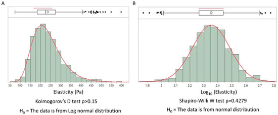
A Universal Model for the Log-Normal Distribution of Elasticity in Polymeric Gels and Its Relevance to Mechanical Signature of Biological TissuesTue Feb 16 2021
#AtomicForceMicroscopy ( #AFM ) is used as an important tool to assess the #elasticproperties of biological samples such as biologicaltissues etc.
In the article “Universal Model for the Log-Normal Distribution of Elasticity in Polymeric Gels and Its Relevance to Mechanical Signature of Biological Tissues* A. Millet proposes a physical model explaining how elasticity values frequently follow a log normal distribution and suggests that distribution-type analysis could increase the information obtained from AFM studies on #biologicaltissues.
NanoAndMore Colloidal #AFMprobes CP-qp-scont-BSG-A-5 were used to assess the elastic properties of the biological samples. The AFM measurements were done in PBS (Phosphate Buffer Saline).
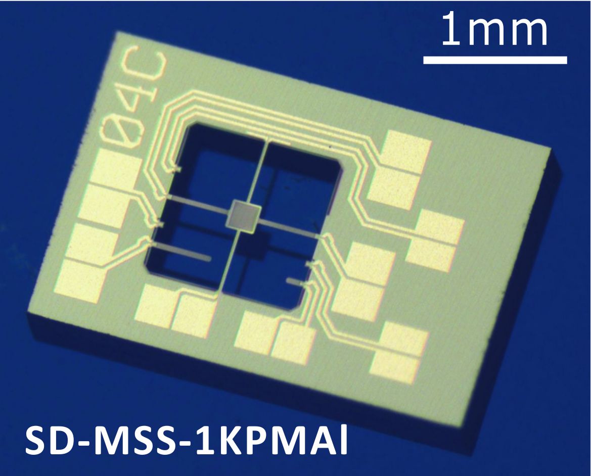
Two New MSS Sensors for Torque Magnetometry added to NANOSENSORS™ Special Developments ListMon Feb 15 2021
Two New MSS Sensors for Torque Magnetometry added to the Special Developments List
NANOSENSORS™ has completed the development of two additional Membrane-type Surface-stress Sensors (MSS) ( SD-MSS-1KPMAl and SD-MSS-1KPMAu ) dedicated for torque magnetometry. Torque magnetometry is a useful technique often employed for assessment of various materials like organic conductors, magnetic and superconductor materials. Now NANOSENSORS™ has added two new types of MSS for this application “SD-MSS-1KPMAl” and “SD-MSS-1KPMAu” to the NANOSENSORS™Special Developments List.
These sensors can be used for nanomechanical sensing, material assessment, static/pulsed-field torque magnetometry, force sensing, and other applications. […]

OPUS 160AC-NG AFM probes used in a recent study.Mon Feb 15 2021
Strain-dependent luminescence and piezoelectricity in monolayer semiconductors studied with the help of our OPUS 160AC-NG AFM probes.

Highlights


AFM Probe Focus

best of the best
qp-HBC
uniqprobe™ - HeartBeat Cantilever for ScanAsyst®** and Peak Force Tapping™**
Coating:
Reflective Aluminum
Tip Shape: Circular symmetric
Tip Shape: Circular symmetric
AFM Cantilever:
F
60 kHz
C
0.5 N/m
L
115 µm
ATEC-NC
Tapping Mode AFM Probe with REAL Tip Visibility
Coating:
none
Tip Shape: Visible
Tip Shape: Visible
AFM Cantilever:
F
335 kHz
C
45 N/m
L
160 µm
TESPA
Standard Tapping Mode AFM Probe
Coating:
Reflective Aluminum
Tip Shape: Standard
Tip Shape: Standard
AFM Cantilever:
F
320 kHz
C
42 N/m
L
125 µm
OTESPA
Standard Tapping Mode AFM Probe with AFM Tip at the Very End of the AFM Cantilever
Coating:
Reflective Aluminum
Tip Shape: Optimized Positioning
Tip Shape: Optimized Positioning
AFM Cantilever:
F
300 kHz
C
26 N/m
L
160 µm