
A protocol to profile the structure and composition of individual EVs with the help of BudgetSensors® gold coated Tap300GB-G AFM probesTue Apr 22 2025
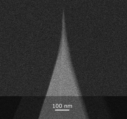
“Extracellular vesicles (EVs) are nanosized particles that… play a key role in intercell communication and are used as transport vehicles for various cell components… We introduce a protocol to profile the structure and composition of individual EVs with the help of atomic force microscopy infrared spectroscopy (AFM-IR), a nanoscale chemical imaging technique” and BudgetSensors® gold coated Tap300GB-G AFM probes.

The samples in this article were scanned in 1 mL folding buffer in AC and HyperDrive mode using NanoWorld d Ultra-Short AFM cantileversMon Apr 14 2025
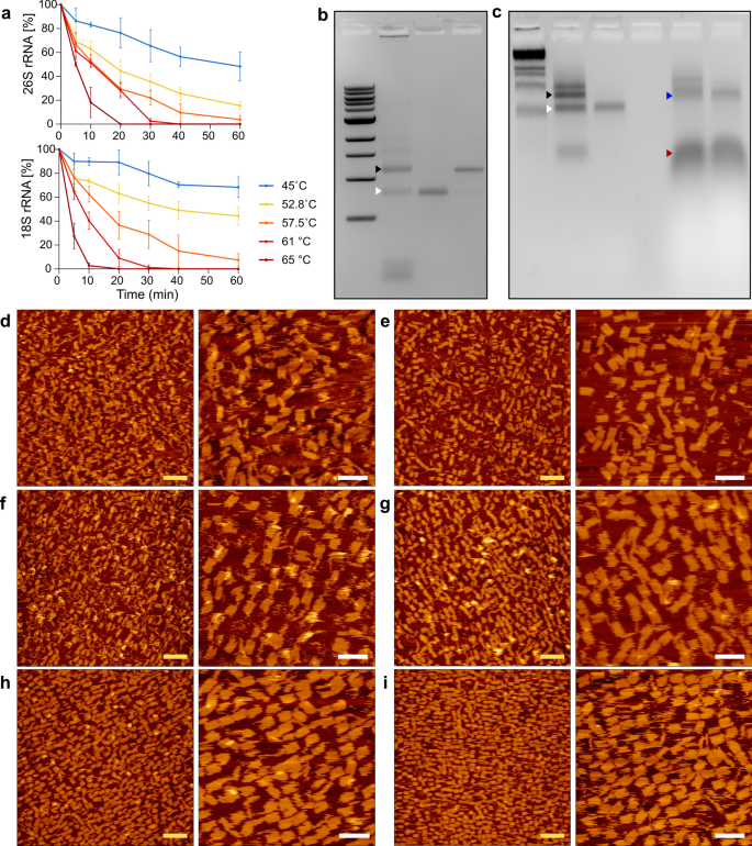
The samples in this article by Anastasia Shapiro et al. (2024 ) were scanned in 1 mL folding buffer in AC and HyperDrive mode using NanoWorld d Ultra-Short AFM cantilevers with force constant 0.3 N/m (USC-F0.3-k0.3 https://www.nanoworld.com/Ultra-Short-Cantilevers-USC-F0.3…
Anastasia Shapiro, Noah Joseph, Nadav Mellul, Almogit Abu-Horowitz, Boaz Mizrahi and Ido Bachelet
Folding molecular origami from ribosomal RNA
Journal of Nanobiotechnology, Volume 22, article number 218, (2024)


Check how NANOSENSORS™ PointProbePlus PPP-NCL AFM cantilevers were used as sensorsFri Apr 11 2025
Check this from NANOSENSORS :
"The room-temperature #ncAFM measurements in this article by Antoine Hinaut et al. (2024), were performed with a home-built noncontact #atomicforcemicroscope and NANOSENSORS PointProbePlus PPP-NCL AFM cantilevers were used as sensors (typical resonance frequencies of f1 = 150 kHz, f2 = 1 MHz, ft = 1.6 MHz, and oscillation amplitudes A1 = 2–5 nm, A2 = 400–800 pm, and At = 40–80 nm for first and second torsional eigenmodes, respectively).
Antoine Hinaut, Sebastian Scherb, Xuelin Yao, Zhao Liu, Yiming Song, Lucas Moser, Laurent Marot, Klaus Müllen, Thilo Glatzel, Akimitsu Narita and Ernst Meyer
Stable Au(111) Hexagonal Reconstruction Induced by Perchlorinated Nanographene Molecules
The Journal of Physical Chemistry C, 2024, 128, 44, 18894–18900
Buy them here: https://www.nanoandmore.com/eu/AFM-Probe-PPP-NCLPt…


"Cell migration plays a key role in physiological processes such as wound healing, immune response, and cancer metastasis."Mon Mar 31 2025
“Eukaryotic cells show an astounding ability to remodel their shape and cytoskeleton and to migrate through pores and constrictions smaller than their nuclear diameter… Here, we study the mechanics and dynamics of mesenchymal cancer cell nuclei transitioning through three-dimensional compliant hydrogel channels. “
CP-PNPL-SiO-B and CP-CONT-PS-B colloidal AFM probes are used to assess the mechanical properties of the hydrogel and the cell nuclei.


Interfacial Engineering with One-Dimensional Lepidocrocite TiO2-Based Nanofilaments for High-Performance Perovskite Solar CellsMon Mar 31 2025
The #photoconductiveatomicforcemicroscopy ( #pcAFM )measurements described in this article were taken in air, using conductive PtIr-coated @NanoWorld Pointprobe® CONTPt silicon #AFMtips. https://www.nanoworld.com/contact-mode-platinum-coated…
Shrabani Panigrahi, Hussein O. Badr, Jonas Deuermeier, Santanu Jana, Elvira Fortunato, Rodrigo Martins and Michel W. Barsoum
Interfacial Engineering with One-Dimensional Lepidocrocite TiO2-Based Nanofilaments for High-Performance Perovskite Solar Cells
ACS Omega 2024, 9, 51, 50820–50829

Conserved structures and dynamics in 5′-proximal regions of Betacoronavirus RNA genomesSat Mar 29 2025
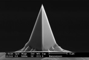
#AFM imaging in tapping mode in air was performed with @NANOSENSORS PointProbe® Plus PPP-NCH #AFMprobes https://www.nanosensors.com/pointprobe-plus-non-contact…
For the liquid experiments the 0.3 N/m #AFMcantilever with 90 kHz resonance frequency of the @NANOSENSORS uniqprobe qp-BioAC https://www.nanosensors.com/uniqprobe-uniform-quality… was used.
Tales Rocha de Moura, Elżbieta Purta, Agata Bernat, Eva M Martín-Cuevas, Małgorzata Kurkowska, Eugene F Baulin, Sunandan Mukherjee, Jakub Nowak, Artur P Biela, Michał Rawski, Sebastian Glatt, Fernando Moreno-Herrero and Janusz M Bujnicki
Conserved structures and dynamics in 5′-proximal regions of Betacoronavirus RNA genomes
Nucleic Acids Research, Volume 52, Issue 6, 12 April 2024, Pages 3419–3432


Looking for elusive quantum particles? Try a bad metal, researchers suggestTue Mar 25 2025
A study of hyperbolic plasmon polaritons in Molybdenum Oxide Dichloride (MoOCl2) with s-SNOM
“Bad metals may make for poor electrical conductors, but it turns out that they make good quantum materials… Bad metals might not be so bad after all.” 

Join us at the American Physical Society, Global Physics Summit 2025Tue Mar 18 2025
Join us at the American Physical Society @Global Physics Summit 2025, taking place from March 16–21 at the Anaheim Convention Center in Anaheim, CA. Visit us at Booth 913 to explore our latest innovation: the SelfAdjust-Air AFM Tips, specifically designed for Bruker’s ScanAsyst® mode.
The APS Global Physics Summit is the largest physics research conference globally, uniting over 14,000 members of the scientific community across all physics disciplines. We look forward to connecting with fellow professionals and discussing advancements in AFM technology.


Poroelastic and viscoelastic properties of soft materials determined from AFM force relaxation and force-distance curvesMon Mar 17 2025
AFM force relaxation and force-distance curves with sQube colloidal AFM probes help study the poroelastic and viscoelastic properties of soft matter.
“The AFM-based methodology described herein provides a solid framework to draw up a complete characterization of the time-dependent mechanical properties of living matter. Due to the structural complexity of cells and tissues, understanding their energy dissipation mechanisms (related to the experimental conditions) is an essential prerequisite toward quantitative determination of their mechanical responses, by analyzing experimental data with the appropriate theoretical models.”


High-Speed Three-Dimensional Scanning Force Microscopy Visualization of Subnanoscale Hydration Structures on Dissolving Calcite Step EdgesMon Mar 17 2025
NanoWorld Ultra-Short Cantilevers USC-F5-k30 https://www.nanoworld.com/Ultra-Short-Cantilevers-USC-F5-k30 for #highspeedatomicforcemicroscopy were used for the high-speed #ThreeDimensionalScanningForceMicroscopy ( #3DSFM ) imaging at 1.5 s/3D image while maintaining F min of 25 pN described in this article:
Kazuki Miyata, Kosuke Adachi, Naoyuki Miyashita, Keisuke Miyazawa, Adam S. Foster and Takeshi Fukuma
High-Speed Three-Dimensional Scanning Force Microscopy Visualization of Subnanoscale Hydration Structures on Dissolving Calcite Step Edges
Nano Letters 2024, 24, 35, 10842–10849

Congratulations to MikroMasch® on the launch of their latest innovation—the SelfAdjust-Air AFM probes!Fri Mar 14 2025
We are proud to announce our brand new SelfAdjust-Air AFM probes.
The SelfAdjust-Air AFM probes are specifically designed for Bruker's ScanAsyst®* mode. The AFM cantilever properties, including the force constant and the Q-factor, optimally support the ScanAsyst®* self-optimization algorithm.
The SelfAdjust-Air are available to order now!
* ScanAsyst® is a trademark of Bruker Corporation

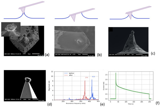
Magnesium Transfer between Atomic Force Microscopy Probes and Metal Electrodes in Aqueous Alginate ElectrolytesThu Mar 13 2025
@NANOSENSORS diamond coated PointProbe® Plus AFM probes CDT-NCHR https://www.nanosensors.com/conductive-diamond-coated-tip… were used for the deposition experiments with an #AFMprobe as an electrode described in this article.
@NANOSENSORS PointProbe® Plus PPP-NCHR #AFMprobes https://www.nanosensors.com/pointprobe-plus-non-contact… were used to examine the deposition results on the on the substrates.
Walter J. Legerstee, Lindah Kiriinya, Mark Kwakernaak and Erik M. Kelder
Magnesium Transfer between Atomic Force Microscopy Probes and Metal Electrodes in Aqueous Alginate Electrolytes
Polymers 2024, 16(12), 1615


50 probes without having to order 50 identical AFM probes - BudgetComboBox from BudgetSensors®Tue Mar 11 2025
Our unique product BudgetComboBox allows you to compile a selection of different AFM probes of your choosing.
With the BudgetComboBox you take advantage of our built-in volume discounts for boxes of 50 probes without having to order 50 identical AFM probes.


Human muscle stem cell responses to mechanical stress into tunable 3D alginate matricesWed Mar 05 2025
Our colloidal probes with glass microspheres support research on human muscle stem cell encapsulation in hydrogels, helping develop higher efficiency muscle regeneration protocols to treat muscle injury.


World Engineering Day for Sustainable Development 2025Tue Mar 04 2025
Happy World Engineering Day for Sustainable Development 2025!
“Engineering has always had an essential role in development and human welfare. Ensuring that future generations of engineers and scientists will be able to design solutions for local and global challenges is critical.
UNESCO's General Conference proclaimed the 4 March World Engineering Day for Sustainable Development during its 40th session in November 2019 (40 C/64), to raise awareness of the role of engineering in modern life, which is essential to mitigate the impact of climate change and advance sustainable development, especially in Africa and the small island developing states (SIDS).”


Nanoscale resolved mapping of the dipole emission of hBN color centers with a scattering-type scanning near-field optical microscopeMon Mar 03 2025
#Colorcenters in #hexagonalboronnitride ( #hBN) are promising candidates as #quantumlightsources for future technologies. *
In the article “Nanoscale resolved mapping of the dipole emission of hBN color centers with a scattering-type scanning near-field optical microscope “, Iris Nihues, Daniel Wigger, Korbinian Kaltenecker, Annika Klein-Hitpass , Philippe Roelli, Aleksandra K. Dąbrowska, Katarzyna Ludwiczak, Piotr Tatarczak , Janne O. Becker , Robert Schmidt, Martin Schnell, Johannes Binder, Andrzej Wysmołek and Rainer Hillenbrand utilize a #scatteringtypeNearfieldOpticalMicroscope ( #sSNOM ) to study the #photoluminescence (PL) emission characteristics of such #quantumemitters in metalorganic vapor phase epitaxy grown hBN. *
On the one hand, Iris Niehues et al. demonstrate direct near-field optical excitation and emission through interaction with the #nanofocus of the #AFMtip resulting in a subdiffraction limited tip-enhanced PL hotspot. *
On the other hand, the authors show that indirect excitation and emission via scattering from the AFM tip significantly increases the recorded PL intensity. This demonstrates that the tip-assisted PL (TAPL) process efficiently guides the generated light to the detector.
Iris Niehues et al. apply the TAPL method to map the in-plane dipole orientations of the hBN color centers on the nanoscale. This work promotes the widely available s-SNOM approach to applications in the quantum domain including characterization and optical control.
The investigation utilizes a scattering-type near-field optical microscope employing a metallized Arrow AFM tip ( NanoWorld Arrow-NCPt #AFMprobehttps://www.nanoworld.com/tapping-mode-platinum-coated-afm-tip-arrow-ncpt ) illuminated by monochromatic laser light.
The AFM tip acts as an #opticalantenna, transforming the incident p-polarizedlight into a highly focused near field at the AFM tip apex, the so-called #nanofocus.
The nanofocus interacts with the sample leading to modified scattering from the AFM tip and encoding local sample properties.
In conventional s-SNOM operation, the elastically scattered light is recorded as function of sample position (note that the sample is scanned), yielding near-field optical images with a spatial resolution down to 10 nm.
To supress background scattering, the AFM is operated in tapping mode and the detector signal is demodulated at a higher harmonic of the AFM tip's oscillation frequency.
Please have a look at the NanoWorld blog for the full citation and a direct link to the full article https://www.nanoworld.com/…/nanoscale-resolved-mapping-of…/


NanoAndMore Japan will be exhibiting at the 72nd Japan Society of Applied Physics Spring Academic Conference and Exhibition JSAP EXPO Spring 2025Fri Feb 28 2025
NanoAndMore Japan will be exhibiting at the 72nd Japan Society of #AppliedPhysics Spring Academic Conference and Exhibition
JSAP EXPO Spring 2025
A representative will be at the booth, so please feel free to contact us with any questions.
Please visit us at our booth to learn all about the #AFMprobes we offer: NanoWorld , NANOSENSORS , Olympus Corporation, nanotools ,BudgetSensoMikroMasch and sQube Colloidal AFM Probes are all available from us.
Date and time:
March 14th (Friday) to 16th (Sunday), 2025 9:30-18:00
March 17th (Monday) 9:30-12:00
Location: Tokyo University of Science Noda Campus Morito Memorial Gymnasium

Thickness-Tunable Zoology of Magnetic Spin Txtures Observed in Fe5GeTe2Thu Feb 27 2025
The family of two-dimensional (2D) van der Waals (vdW) materials provides a playground for tuning structural and magnetic interactions to create a wide variety of spin textures. *
Of particular interest is the ferromagnetic compound #Fe5GeTe2 that Ajesh K. Gopi et al. show displays a range of complex spin textures as well as complex crystal structures. *
In the article “Thickness-Tunable Zoology of Magnetic Spin Textures Observed in Fe5GeTe2”, using a high-brilliance laboratory X-ray source, Ajesh K. Gopi, Abhay K. Srivastava, Ankit K. Sharma, Anirban Chakraborty, Souvik Das, Hakan Deniz, Arthur Ernst, Binoy K. Hazra, Holger L. Meyerheim and Stuart S.P. Parkin show that the majority (1 × 1) Fe5GeTe2 (FGT5) phase exhibits a structure that was previously considered as being centrosymmetric but rather lacks inversion symmetry. *
In addition, FGT5 exhibits a minority phase that exhibits a long-range ordered (√3 × √3)-R30° superstructure. This superstructure is highly interesting in that it is innately 2D without any lattice periodicity perpendicular to the vdW layers, and furthermore, the superstructure is a result of ordered Te vacancies in one of the topmost layers of the FGT5 sheets rather than being a result of vertical Fe ordering as earlier suggested. *
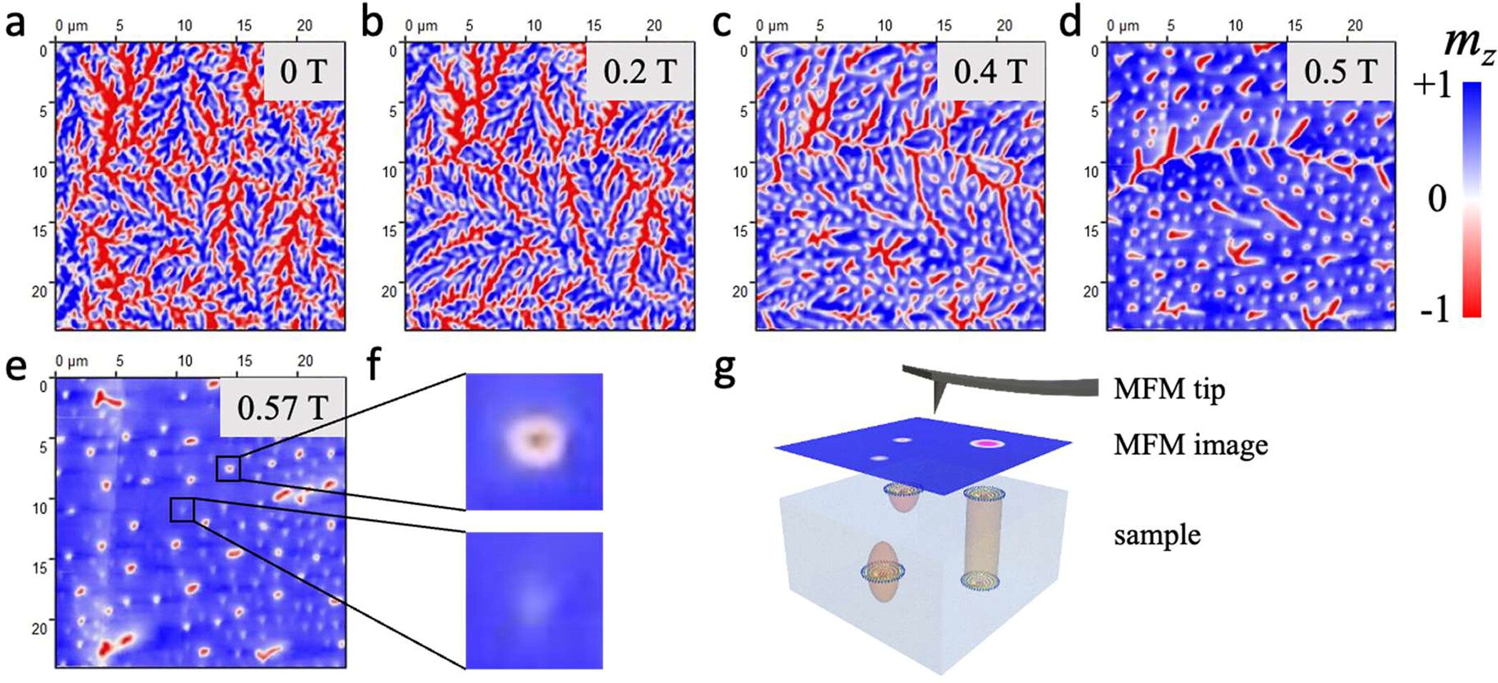
Ajesh K. Gopi et al. show, from direct real-space magnetic imaging, evidence for three distinct magnetic ground states in lamellae of FGT5 that are stabilized with increasing lamella thickness, namely, a multidomain state, a stripe phase, and an unusual fractal state.*
In the stripe phase the authors also observe unconventional type-I and type-II bubbles where the spin texture in the central region of the bubbles is nonuniform, unlike conventional bubbles.
In addition, they find a #bobber or a cocoon-like spin texture in thick (∼170 μm) FGT5 that emerges from the fractal state in the presence of a magnetic field.
Among all the #2DvdW magnets Ajesh K. Gopi et al. have thus demonstrated that FGT5 hosts perhaps the richest variety of magnetic phases that, thereby, make it a highly interesting platform for the subtle tuning of magnetic interactions.
#MagneticForceMicroscopy ( #MFM) measurements were performed in a commercially available variable-temperature #magneticforcemicroscope equipped with a vector superconducting magnet.
NANOSENSORS SSS-MFMR https://www.nanosensors.com/supersharpsilicon-magnetic…, a magnetic #AFMprobe with an #AFMtip radius of curvature < 15 nm was used for all MFM measurements.
Please have a look at the NANOSENSORS blog for the full citation and a direct link to the full article

Visit us at NanoAndMore USA booth no. 408 at the Biophysical Society meeting 2025Fri Feb 14 2025
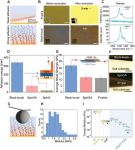
Durable and conductive interfaces that enable chronic and high-resolution recording of neural activity are essential for understanding and treating #neurodegenerativedisorders. These #chronicimplants require long-term stability and small contact areas. Consequently, they are often coated with a blend of conductive #polymers and are crosslinked to enhance durability despite the potentially deleterious effect of crosslinking on the mechanical and electrical properties.
In the article “Surface-Grafted Biocompatible Polymer Conductors for Stable and Compliant Electrodes for Brain Interfaces” by Rachel Blau, Samantha M. Russman, Yi Qie, Wade Shipley, Allison Lim, Alexander X. Chen, Audithya Nyayachavadi, Louis Ah, Abdulhameed Abdal, Guillermo L. Esparza, Samuel J. Edmunds, Ritwik Vatsyayan, Sean P. Dunfield, Moumita Halder, Jesse V. Jokerst, David P. Fenning, Andrea R. Tao, Shadi A. Dayeh and Darren J. Lipomi (2024) https://advanced.onlinelibrary.wiley.com/…/adhm.202402215
Describe the grafting of the poly(3,4 ethylenedioxythiophene) scaffold, poly(styrenesulfonate)-b-poly(poly(ethylene glycol) methyl ether methacrylate #blockcopolymerbrush to gold, in a controlled and tunable manner, by surface-initiated atom-transfer radical polymerization (SI-ATRP). This “#blockbrush ” provides high volumetric capacitance (120 F cm─3), strong adhesion to the metal (4 h ultrasonication), improved surface hydrophilicity, and stability against 10 000 charge–discharge voltage sweeps on a multiarray neural electrode. In addition, the block-brush film showed 33% improved stability against current pulsing. This approach can open numerous avenues for exploring specialized polymer brushes for bioelectronics research and application.
The following #AFMprobes offered by NanoAndMore were used for the #AFMcharacterization described in the article:
The #topographical imaging was done with MikroMasch Opus 160AC NA #AFMtips for #tappingmode in air https://www.nanoandmore.com/AFM-Tip-160AC-NA and NANOSENSORS uniqprobe qp-BioAC #AFMtips https://www.nanoandmore.com/AFM-Probe-qp-BioAC for #liquidimaging in DI water.
The #mechanicalmeasurements were conducted in DI water with nanotools Biosphere B500-CONT #AFMtips https://www.nanoandmore.com/AFM-Probe-biosphere-B500-CONT and #indentationcurves were fit to the Dimitriadis model using custom MATLAB scripts.
The thickness of the brush for the model fitting was found by scraping away an area of brush in air with a MikroMasch HQ:NSC14/Hard/Al BS #AFMtip https://www.nanoandmore.com/AFM-Probe-hq-nsc14-hard-al-bs , leaving behind the bare gold substrate, washing, and measuring the height of the neighboring brushes in tapping mode after equilibration in water for 1 h.
Want to find out more about these #AFMcantilevers? Then visit us at NanoAndMore USA booth no. 408 at the @@Biophysical Society meeting 2025 #bps in Los Angeles from February 16-18, 2025 https://www.biophysics.org/2025meeting

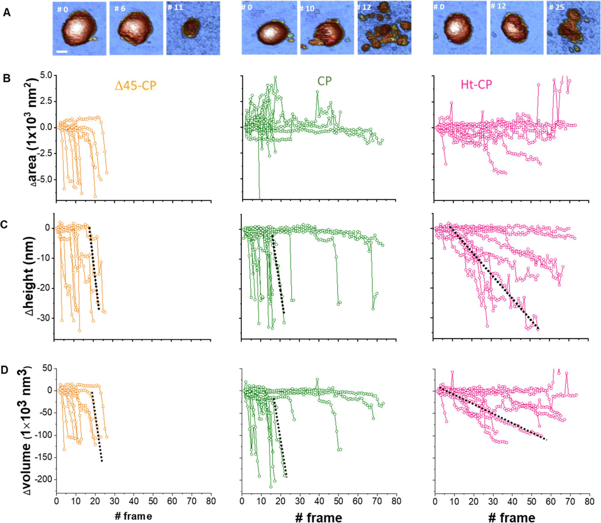
Mechanical disassembly of human picobirnavirus like particles indicates that cargo retention is tuned by the RNA-coat protein interactionWed Feb 12 2025
The idea of using #viruslikeparticles as #nanocarriers for #heterologouscargotransport and delivery requires controlling the stability of the container–cargo system. *
In particular, the conditions of the cargo delivery entail tailoring the escape of the molecular payload when the #virusparticle is disassembled. What happens to the internalized molecules when the #nanocage is opened? *
To this end, it is necessary to control the cargo–container interaction which, in turn, would tune the retention of cargo when the disassembly of the #nanocarrier takes place. Thus, it is necessary to develop nanocarrier systems that facilitate the control of the cargo retention conditions as a function of its interaction with the #nanocontainer. *
In the article “Mechanical disassembly of human picobirnavirus like particles indicates that cargo retention is tuned by the RNA–coat protein interaction” María J. Rodríguez-Espinosa, Javier M. Rodríguez, José R. Castón and Pedro J. de Pablo describe how they designed three mutants of human #picobirnavirus where the #RNA–coat protein interaction, observed previously via cryo-electron microscopy, is modified by changing the N-terminal end of the coat protein.
The authors used #atomicforcemicroscopy ( #AFM) for inducing the mechanical unpacking of the #RNA internalized in particles of each mutant. *
Their experiments crack-opened individual particles in real time to monitor the cargo release. Among other results, María J. Rodríguez-Espinosa et al. have measured that an increment in the N-terminal length by just 8% increases the cargo retention of partially disrupted particles by a factor of 10 with respect to the wild type. *
For #mechanicalfatigue experiments, rectangular #AFMcantilevers ( NANOSENSORS™, uniqprobe qp-BioAC #AFMprobes with three different AFM cantilevers per chip) with nominal spring constants of 0.05 and 0.1 N m−1 were used. https://www.nanosensors.com/uniqprobe-uniform-quality…
Please visit the NANOSENSORS blog for the full citation and a direct link to the full article.


