
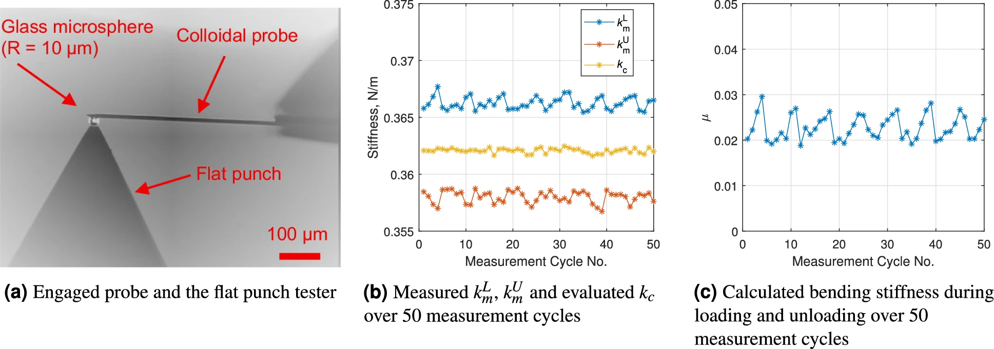
Traceable stiffness calibration of colloidal AFM probes for biomechanical measurementsMon Jul 06 2026
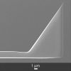
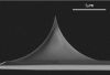
In their recent report Li et al. look at frictional effects in AFM indentation measurements. The paper employs FEA studies, in addition to AFM indentation. Capturing this effect is vital for accurate and traceable calibration of AFM probes. CP-CONT-BSG-C is among the models used!
Read Here: https://www.nature.com/articles/s41598-026-38158-7#Sec2

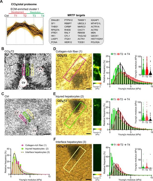
Dynamics of Compartment-Specific Proteomic Landscapes of Hepatotoxic and Cholestatic Models of Liver FibrosisThu May 21 2026
Liver fibrosis is characterized by excessive accumulation and remodeling of extracellular matrix (ECM) components, leading to altered tissue mechanics and progressive impairment of liver function. In this article, Marketa Jirouskova, Karel Harant, Pavel Cejnar, Srikant Ojha, Katerina Korelova, Lenka Sarnova, Eva Sticova, Christoph H. Mayr, Herbert B. Schiller, and Martin Gregor investigate compartment-specific proteomic remodeling during fibrosis progression and spontaneous healing in experimental mouse models of hepatotoxic and cholestatic liver injury.
Using detergent-based tissue extraction combined with mass spectrometry, the authors identified dynamic and etiology-specific changes in the hepatic proteome with particular focus on extracellular matrix composition and protein solubility. Distinct molecular signatures associated with carbon tetrachloride (CCl4)-induced and DDC-induced fibrosis were observed, including signaling pathways linked to impaired healing and carcinogenesis in cholestatic injury. The extracellular chaperone clusterin was additionally identified as a potential contributor to fibrosis resolution.
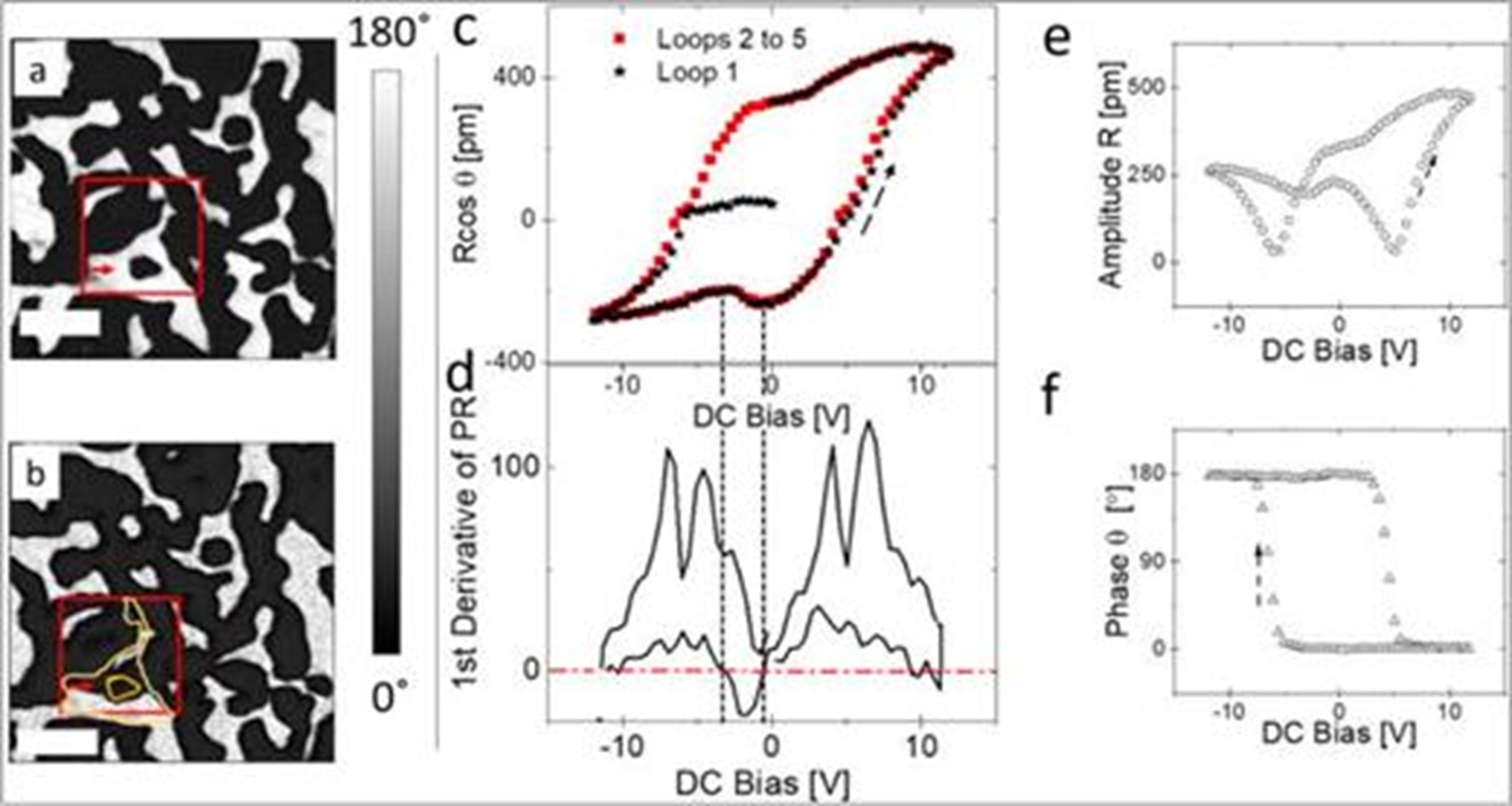
Negative Differential Piezoresponse in Relaxor FerroelectricsThu Apr 23 2026
Relaxor ferroelectrics exhibit complex electromechanical responses that are critical for advanced functional materials. In this article, C. Saguy, B. Kowalski, A. Sehirlioglu, and Y. Ivry report non-ergodic-induced negative differential piezoresponse behavior.
Piezoresponse force microscopy (PFM) was used to investigate domain switching and nanoscale electromechanical properties. The study reveals unconventional polarization responses associated with non-ergodic states. Measurements were carried out using a NanoSensors PtSi-FM AFM probe with a force constant of 2.5 N/m and a resonance frequency of 70 kHz. The AFM probe enabled high-resolution imaging, domain writing, and switching spectroscopy under controlled bias conditions.
This work highlights the role of NanoSensors AFM probes in enabling precise characterization of complex ferroelectric phenomena at the nanoscale.

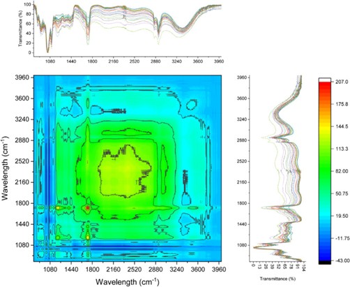
Structural Elucidation of Citric Acid Cross-Linked Pectin and Its Impact on the Properties of Nanocellulose-Reinforced Packaging FilmsWed Apr 15 2026
Citric acid cross-linking is an effective strategy for modifying citrus pectin to enhance its performance in sustainable packaging applications. In this article, Chandra Mohan Chandrasekar, Daniele Carullo, Francesco Saitta, Tommaso Bellesia, Elena Caneva, Chiara Baschieri, Marco Signorelli, Dimitrios Fessas, Stefano Farris and Davide Romano, investigated the structural changes induced by citric acid cross-linking and their influence on the properties of nanocellulose-reinforced packaging films..
The authors demonstrated that cross-linking significantly alters the structure–property relationship of the biopolymer matrix, leading to improved film integrity and modified surface morphology. These results provide valuable insight into biopolymer modification strategies for the development of environmentally friendly packaging materials.

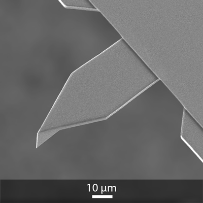
Did you know, OPUS by MikroMasch® product line features the 55AC AFM probes?Wed Apr 15 2026
Did you know, OPUS by MikroMasch® product line features the 55AC AFM probes? These probes are designed for high-frequency AFM applications along with a tip located precisely at the cantilever free end, allowing for accurate positioning over the sample!
You find them with us here: https://www.nanoandmore.com/search/products?term=55ac
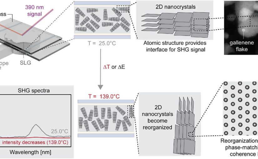
Nonlinear Optical Response in Layer-Stacked Gallenene with Ferroelectric PolarizationMon Mar 30 2026
Layer-stacked gallenene is an emerging two-dimensional material with unique structural and electronic propertiesIn this article, M.Yunusa, A. K.Schulz, T.Parker, et al. investigated the nonlinear optical response of layer-stacked gallenene exhibiting ferroelectric polarization. The material was produced using a liquid metal-based synthesis approach and showed a phase transition associated with its stacked structure.
The authors demonstrated strong second harmonic generation (SHG) signals, revealing the nonlinear optical activity of gallenene and confirming its ferroelectric nature. These findings highlight the potential of gallenene as a novel functional 2D material for advanced optoelectronic and photonic applications.
Atomic force microscopy (AFM) was used to characterize transparent lamellar films and helical filaments. Measurements were performed using a commercially available AFM instrument operated in contact mode. A NanoWorld Arrow-CONTR AFM probe with a nominal force constant of 0.2 N/m and a resonance frequency of 14 kHz was used to obtain high-resolution surface morphology data.
New NANOSENSORS™ blog postThu Mar 26 2026
Thermal deflection analysis in AFM for precise nanomechanical property measurements — validated on HOPG using a range of NANOSENSORS probes.


NanoAndMore Japan at The 73rd JSAP Spring Meeting 2026Mon Mar 16 2026
NanoAndMore Japan is at The 73rd JSAP Spring Meeting 2026 03 15-18
You can find us at Booth NO.1-27

 were used in the characterization experiments during development of the AI approach")
BudgetSensors® Multi75E-G tips, (a.k.a. ElectriMulti75) were used in the characterization experiments during development of the AI approachTue Feb 17 2026
AFM and scanning probe microscopy in general have become ubiquitous since their discovery. However, analyzing and acquiring data frequently involves operator judgement in selecting and focusing on regions. In this recent publication, Sung et al. demonstrate an autonomous, AI-based framework for microstructural and electrical analysis of 2D materials.
Our Multi75E-G tips, (a.k.a. ElectriMulti75) were used in the characterization experiments during development of the AI approach.
Read the full article here: https://doi.org/10.1002/sstr.202500379
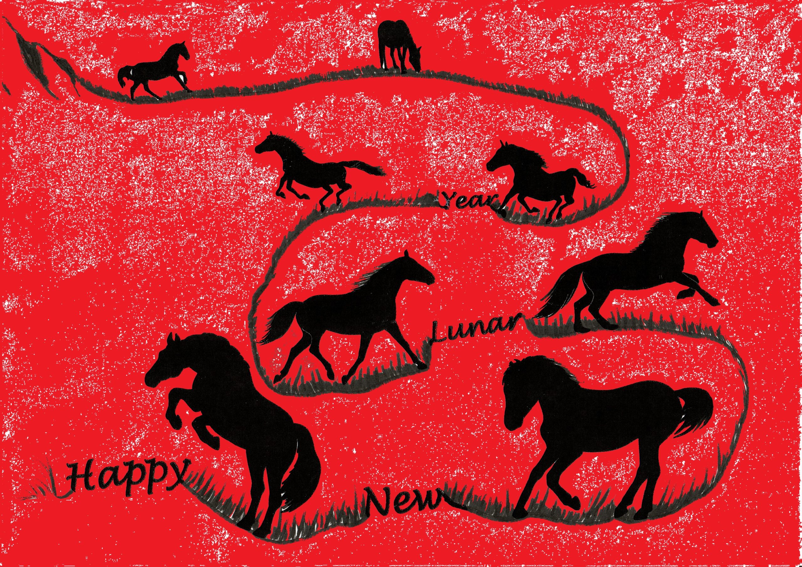
Happy New Lunar Year of the HorseMon Feb 16 2026
NANOSENSORS™ AFM probes wishes you all a happy, healthy and successful new lunar year of the horse.

Happy New Lunar Year of the HorseMon Feb 16 2026
NanoWorld® wishes everyone a good start into the new lunar year of the horse.

BudgetSensors® Multi75Al-G probe has been used to image the polydopamine coating morphologyMon Jan 26 2026
In a recent study, Frenzel et al. demonstrated optimized polydopamine coatings for polyethylene fibers in cementitious materials. Short fibers have been demonstrated as an effective means of reinforcing this class of materials previously, when the correct adhesion between the fiber and the surrounding matrix is achieved.
BudgetSensors® Multi75Al-G probe has been used to image the polydopamine coating morphology – a thin film with nanoscale clusters on top.
https://www.sciencedirect.com/…/arti…/pii/S0169433225016137…
#BudgetSensors #AFMprobes #AFMtips #Multi75AlG

Season’s Greetings 2025 from NanoWorld®Tue Dec 23 2025
As we glide toward the end of the year, we’d like to say a heartfelt thank you to our customers and partners around the world for trusting NanoWorld AFM probes in your research and industry related applications.
Whether you’re carving fresh tracks like the NanoWorld Professor or enjoying the view like our robot friend in the gondola in this year’s holiday cartoon, we hope this festive season brings you inspiration, well-earned rest, and exciting discoveries ahead. ☃️⛷️🚠
✨ Wishing you a joyful Christmas and a successful, curiosity-driven New Year 2026! ✨
We look forward to continuing the journey together in the year to come.

Happy Holidays 2025 from NANOSENSORS™ AFM ProbesMon Dec 22 2025
As the year slowly but surely comes to a close, we would like to wish all users of our #AFMprobes a joyful holiday season.
This year, we’re celebrating a little differently—not with the picture of a traditional Christmas tree, but with a festive Christmas Tree Merry-Go-Round 
 .
.
We wish you a relaxing holiday season and a successful start to the new year.
Thank you for your continued trust and collaboration.
We look forward to working together with you in 2026. 

NanoAndMore USA is at MRS Fall 2025!Thu Nov 27 2025
@NanoAndMore USA is at MRS Fall 2025!
Visit us at Booth #411 at the Materials Research Society (MRS) Fall Exhibit at Hynes Convention Center in Boston https://www.mrs.org/…/2025-mrs…/exhibit---sponsor/attendees and be among the first to discover the new MikroMasch SelfAdjust-Air AFM probes https://www.nanoandmore.com/AFM-Probe-selfadjust-air-for… and the newly introduced NanoWorld Arrow-ACR probes https://www.nanoandmore.com/AFM-Probe-ARROW-ACR.
As your trusted supplier for #AFMprobes for every application, we’re here to help you choose the ideal probe for your research—no matter whether you're working in #topography, #biomaterials, #softmaterials, #conductiveAFM, #2Dmaterials or other #materialsresearch areas.
Stop by Booth #411, meet the NanoAndMore USA team, and let’s find the perfect AFM probe to power your next breakthrough!

NanoAndMore Europe proudly sponsors the XIII Workshop on Applications of Scanning Probe Microscopy – STM/AFM 2025Tue Nov 25 2025
NanoAndMore Europe proudly sponsors the XIII Workshop on Applications of Scanning Probe Microscopy – STM/AFM 2025, which will be held in Zakopane from 26 - 30 November 2025 https://nanosam.pl/stmafm2025/
The Workshop is organized by the Centre for Nanometer-scale Science and Advanced Materials (NANOSAM) https://nanosam.pl/ of the Faculty of Physics, Astronomy, and Applied Computer Sciences, Jagiellonian University in Krakow, Poland.
Unfortunately, we are unable to attend in person this year, but we encourage all participants to look at our #AFMprobes flyer in the conference bag for the latest updates and offers from NanoAndMore.
If you have any questions on the #AFMtips by BudgetSensors, MikroMasch, OPUS, NanoWorld, NANOSENSORS, nanotools, sQube Colloidal AFM Probes and original Olympus #microcantilvers we offer, please free to contact us.
The NanoAndMore team wishes the organizers and all attendees a successful workshop filled with inspiring scientific exchange. A quick look at the webcam on Krupowki Street shows that there is plenty of snow in Zakopane this year, making the non-scientific activities especially appealing!
#nanoandmore #scanningprobemicroscopy #atomicforcemicroscopy #nanoscience #AFM #SPM #nanoscale #nanoscience #appliedphysics #materialsscience #materialsreserach #AFMtips #SPMtips #NANOSAM

NEW – NanoWorld® introduces Arrow-ACR Silicon AFM probeMon Nov 10 2025
Looking for a reliable replacement for the discontinued OLYMPUS® AC160 #microcantilever?
The NanoWorld® Arrow™ ACR #AFMprobe offers identical mechanical properties combined with the well-known Arrow series features of enhanced tip visibility and optimized positioning accuracy. Perfect for non-contact and Tapping™ mode studies of #softmaterials, #thinfilms, #coatings and more.
Discover the Arrow™ ACR – precision engineered for consistent, high-quality AFM results.
CLICK HERE FOR DETAILED INFO ON Arrow™ ACR - https://www.nanoworld.com/tapping-mode-reflex-coated-afm-tip-arrow-acr
NanoWorld® blogpost about Arrow™ ACR - https://www.nanoworld.com/…/new-nanoworld-introduces-arrow…/
All NanoWorld® Arrow AFM Tips - https://www.nanoworld.com/arrow-afm-tips
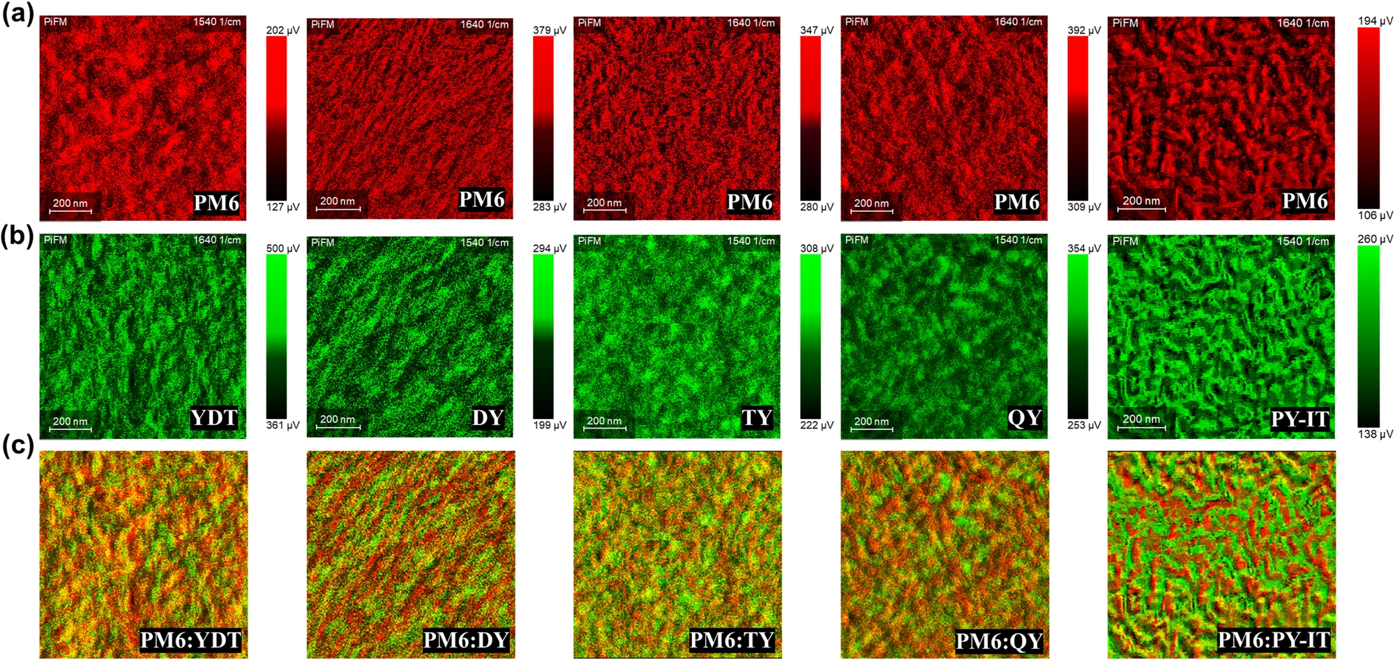
NANOSENSORS™ AFM Probes Enable Nanoscale Insights into Organic PhotovoltaicsFri Oct 10 2025
In their 2023 Nature Communications article, “Precise synthesis and photovoltaic properties of giant molecule acceptors,”Hongmei Zhuo, Xiaojun Li, Jinyuan Zhang, Can Zhu, Haozhe He, Kan Ding, Jing Li, Lei Meng, Harald Ade, and Yongfang Li report a transformative advance in organic solar cell design. By precisely linking multiple small-molecule acceptors into “giant molecule acceptors” (GMAs), the researchers enhanced exciton diffusion and charge transport. Their three-unit GMA reached an impressive power conversion efficiency of 16.32%, highlighting how molecular architecture directly influences photovoltaic performance.
Read the full article here: https://www.nanosensors.com/blog/nanosensors-afm-probes-enable-nanoscale-insights-into-organic-photovoltaics/

Happy National Nanotechnology Day!Thu Oct 09 2025
Celebrating science at the scale of 10⁻⁹ meters — where the smallest innovations create the biggest impact.
There’s hardly a better day in the year to capture some beautiful #AFM images and celebrate the tools that make nanoscience possible. At NanoAndMore USA, we’re proud to support researchers worldwide with the industry’s widest selection of #AFMprobes — trusted by leading labs, universities, and manufacturers across the globe!
#1 AFM Tips Shop Worldwide - https://www.nanoandmore.com/
#AFM #AFMProbes #Nanotechnology #NationalNanotechDay #10Eminus9 #Nano #AtomicForceMicroscopy
Highlights


AFM Probe Focus

best of the best
qp-HBC
uniqprobe™ - HeartBeat Cantilever for ScanAsyst®** and Peak Force Tapping™**
Coating:
Reflective Aluminum
Tip Shape: Circular symmetric
Tip Shape: Circular symmetric
AFM Cantilever:
F
60 kHz
C
0.5 N/m
L
115 µm
ATEC-NC
Tapping Mode AFM Probe with REAL Tip Visibility
Coating:
none
Tip Shape: Visible
Tip Shape: Visible
AFM Cantilever:
F
335 kHz
C
45 N/m
L
160 µm
TESPA
Standard Tapping Mode AFM Probe
Coating:
Reflective Aluminum
Tip Shape: Standard
Tip Shape: Standard
AFM Cantilever:
F
320 kHz
C
42 N/m
L
125 µm
OTESPA
Standard Tapping Mode AFM Probe with AFM Tip at the Very End of the AFM Cantilever
Coating:
Reflective Aluminum
Tip Shape: Optimized Positioning
Tip Shape: Optimized Positioning
AFM Cantilever:
F
300 kHz
C
26 N/m
L
160 µm