Latest News

NanoWorld Real-Time Observation of Fibrous Zeolites Reactivity in Contact with Simulated Lung Fluids (SLFs) Obtained by Atomic Force Microscope (AFM) - news

Real-Time Observation of Fibrous Zeolites Reactivity in Contact with Simulated Lung Fluids (SLFs) Obtained by Atomic Force Microscope (AFM)Wed Sep 04 2019

New post - Real-Time Observation of Fibrous Zeolites Reactivity in Contact with Simulated Lung Fluids (SLFs) Obtained by Atomic Force Microscope (AFM) has been published on NanoWorld Blog.

https://www.nanoworld.com/blog/

Inhalation of fibrous erionite particles has been linked to malignant mesothelioma. Accordingly, erionite is considered the most carcinogenic mineral. The reactivity and the nature of erionite biotoxicity has been the subject of intensive research. Despite very close chemical and structural relationships between erionite and offretite, the reactivity of offretite in lung fluids remains unknown.* In their paper “Real-Time Observation of Fibrous Zeolites Reactivity in Contact with Simulated Lung Fluids (SLFs) Obtained by Atomic Force Microscope (AFM)”, Matteo Giordani, Georgia Cametti, Fulvio Di Lorenzo and Sergey V. Churakov investigate the interaction of erionite and offretite surfaces with simulated lung fluids by means of in situ atomic force microscope (AFM).* The outcomes presented in the paper mentioned above represent an important step in understanding the complex processes occurring at the surfaces of mineral fibres that could be involved in the toxicological pathway.* The topography scans were performed in tapping mode with a NanoWorld Arrow-UHFAuD https://www.nanoworld.com/ultra-high-frequency-afm-tip-arrow-uhf-aud AFM probes under different experimental conditions. To better discriminate the role of the tip from the actual fluid-surface interaction, additional measurements were performed in air and in water in contact mode using an Al-coated NanoWorld Arrow-CONTR https://www.nanoworld.com/contact-mode-reflex-coated-afm-tip-arrow-contr AFM cantilever. Please have a look at the NanoWorld blog for the full citation and a direct link to the full paper. #offretite #biotoxicity #SurfaceInteraction #AtomicForceMicroscopy

NanoAndMore NAM-News-NoImageFill.JPG

NanoAndMore ジャパン がJASIS 2019に出展Tue Sep 03 2019

NanoAndMore ジャパン がJASIS 2019に出展
JASIS2019(9月4日~6日 幕張メッセ)にてNanoWorldホールティング傘下のカンチレバーの展示を行います。6ホールブース6A-402でお待ちしております!

NANOSENSORS A tension-adhesion feedback loop in plant epidermis – NANOSENSORS™ Blog - news

A tension-adhesion feedback loop in plant epidermis – NANOSENSORS™ BlogSun Sep 01 2019

Published new post (A tension-adhesion feedback loop in plant epidermis) on NANOSENSORS™ Blog Mechanical forces have emerged as coordinating signals for most cell functions. Yet, because forces are invisible, mapping tensile stress patterns in tissues remains a major challenge in all kingdoms.* In their research paper “A tension-adhesion feedback loop in plant epidermis” Stéphane Verger, Yuchen Long, Arezki Boudaoud and Olivier Hamant take advantage of the adhesion defects in the Arabidopsis mutant quasimodo1 (qua1) to deduce stress patterns in tissues.* Using suboptimal water potential conditions, the authors revealed the relative contributions of shape- and growth-derived stress in prescribing maximal tension directions in aerial tissues. Consistently, the tension patterns deduced from the gaping patterns in qua1 matched the pattern of cortical microtubules, which are thought to align with maximal tension, in wild-type organs. Conversely, loss of epidermis continuity in the qua1mutant hampered supracellular microtubule alignments, revealing that coordination through tensile stress requires cell-cell adhesion.* Based on the results achieved with plants presented in this research paper, the analysis of basement membrane continuity, and its disruption, may very well help understand how consistent supracellular epidermal patterns relate to mechanical stress, in parallel to the well-established role of cadherin and stress in cell-cell adhesion and epidermal functions.* NANOSENSORS™ special development Sphere AFM probes ( SD-Sphere-NCH-S ) with 400 nm tip radius and 42 N/m spring constant were used. https://www.nanosensors.com/pdf/SpecialDevelopmentsList.pdf Please have a look at the NANOSENSORS blog for the full citation and a direct link to the ful article. https://www.nanosensors.com/pdf/SpecialDevelopmentsList.pdf Please have a look at the NANOSENOSRS blog for the full citation and a direct link to the full article. #CellStiffness #microtubules #AtomicForceMicroscopy #nanoindentation

NanoWorld Launching of hyperbolic phonon-polaritons in h-BN slabs by resonant metal plasmonic antennas - news

Launching of hyperbolic phonon-polaritons in h-BN slabs by resonant metal plasmonic antennasWed Aug 28 2019

New post - Launching of hyperbolic phonon-polaritons in h-BN slabs by resonant metal plasmonic antennas has been published on NanoWorld Blog.

https://www.nanoworld.com/blog/

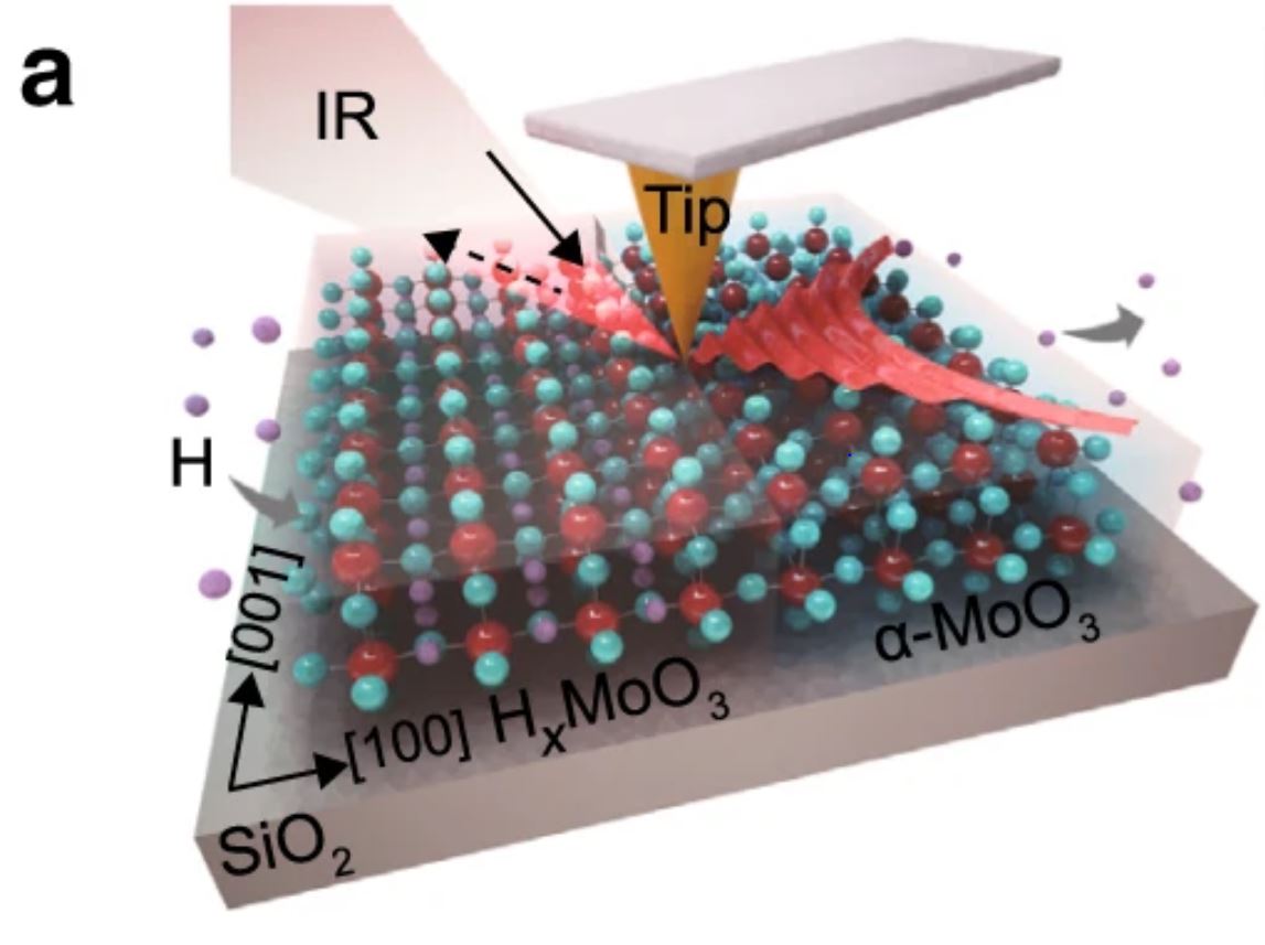
Launching and manipulation of polaritons in van der Waals materials offers novel opportunities for applications such as field-enhanced molecular spectroscopy and photodetection.* Particularly, the highly confined hyperbolic phonon polaritons (HPhPs) in h-BN slabs attract growing interest for their capability of guiding light at the nanoscale. An efficient coupling between free space photons and HPhPs is, however, hampered by their large momentum mismatch.* In the article “Launching of hyperbolic phonon-polaritons in h-BN slabs by resonant metal plasmonic antennas” P. Pons-Valencia, F. J. Alfaro-Mozaz, M. M. Wiecha, V. Biolek, I. Dolado, S. Vélez,P. Li, P. Alonso-González, F. Casanova, L. E. Hueso, L. Martín-Moreno, R. Hillenbrand and A. Y. Nikitin show that resonant metallic antennas can efficiently launch HPhPs in thin h-BN slabs. Despite the strong hybridization of HPhPs in the h-BN slab and Fabry-Pérot plasmonic resonances in the metal antenna, the efficiency of launching propagating HPhPs in h-BN by resonant antennas exceeds significantly that of the non-resonant ones. Their results provide fundamental insights into the launching of HPhPs in thin polar slabs by resonant plasmonic antennas, which will be crucial for phonon-polariton based nanophotonic devices.* A commercial s-SNOM setup in which the oscillating (at a frequency Ω≅270kHz) metal-coated (Pt/Ir) AFM tip (NanoWorld ARROW-NCPt) was illuminated by p-polarized mid-IR radiation, was used.* https://www.nanoworld.com/tapping-mode-platinum-coated-afm-tip-arrow-ncpt Please have a look the NanoWorld blog for the full citation and a direct link to the full paper.

NANOSENSORS Conductive-probe atomic force microscopy and Kelvin-probe force microscopy characterization of OH-terminated diamond (111) surfaces with step-terrace structures - news

Conductive-probe atomic force microscopy and Kelvin-probe force microscopy characterization of OH-terminated diamond (111) surfaces with step-terrace structuresSun Aug 18 2019

Published new post (Conductive-probe atomic force microscopy and Kelvin-probe force microscopy characterization of OH-terminated diamond (111) surfaces with step-terrace structures) on NANOSENSORS Blog Diamond has a high breakdown field, high carrier mobilities and the highest thermal conductivity. That is why diamond is a promising material for next generation high-power devices such as field effect transistors.* In their paper “Conductive-probe atomic force microscopy and Kelvin-probe force microscopy characterization of OH-terminated diamond (111) surfaces with step-terrace structures”, Masatsugu Nagai, Ryo Yoshida, Tatsuki Yamada, Taira Tabakoya, Christoph E. Nebel, Satoshi Yamasaki, Toshiharu Makino, Tsubasa Matsumoto, Takao Inokuma and Norio Tokuda report about a detailed characterization of OH-terminated diamond (111) surfaces with step-terrace (ST) and bunching-step (BS) regions. In order to obtain the OH-terminated diamond (111) surfaces, they combined three techniques: anisotropic diamond etching by thermochemical reaction between Ni and diamond in high-temperature water vapor, hydrogen plasma treatment24) and water vapor annealing. For characterization of the topography as well as electronic surface properties, atomic force microscopy (AFM), Kelvin-probe force microscopy (KPFM) and conductive-prove AFM (CPAFM) were applied.* They found that the contact potential difference (CPD) and current were highly correlated with the surface topography and concluded that the interface states were generated around steps on the OH-terminated diamond (111) surfaces.* The results presented in this paper indicate that atomically flat diamond surfaces with minimal step densities are required to form ideal MOS structures with minimized interface state densities.* The CPD maps of the OH-terminated diamond (111) surfaces were obtained by the KPFM measurements, using NANOSENSORS™ Platinum Silicide ( PtSi ) AFM probes. * https://www.nanosensors.com/uploads/media/files/0001/05/46425f364ed11a0a90b5c6db11118a319a4b4705.pdf Please have a look at the NANOSENORS blog for the full citation and a direct link to the full article. #KPFM #AtomicForceMicroscopy #ScanningProbeMicroscopy
NANOSENSORS Meet NANOSENSORS at booth 218 at ChinaNano 2019 Beijing August 17... - news

Meet NANOSENSORS at booth 218 at ChinaNano 2019 Beijing August 17...Sat Aug 17 2019

We are at booth 218 at the ChinaNano 2019, the 8th International Conference on Nanoscience and Technology at the Beijing International Convention Center (BICC). We are looking forward to seeing you there! Learn all about NANOSENSORS AFM probes at the... #AFMcantilever
#AFMProbes #AFMprobes

NANOSENSORS Meet NANOSENSORS at booth 218 at ChinaNano 2019 Beijing August 17 – 19, 2019 - news

Meet NANOSENSORS at booth 218 at ChinaNano 2019 Beijing August 17 – 19, 2019Sat Aug 17 2019

Published new post (Meet NANOSENSORS at booth 218 at ChinaNano 2019 Beijing August 17 – 19, 2019) on NANOSENSORS Blog We are at booth 218 at the ChinaNano 2019, the 8th International Conference on Nanoscience and Technology at the Beijing International Convention Center (BICC). We are looking forward to seeing you there! Learn all about NANOSENSORS AFM probes at the ChinaNano 2019 #nanotechnology #nanomaterials #AFMcommunity

NanoWorld ChinaNano 2019 Beijing August 17-19, Booth 218 - news

ChinaNano 2019 Beijing August 17-19, Booth 218Sat Aug 17 2019

New post - ChinaNano 2019 Beijing August 17-19, Booth 218 (https://www.nanoworld.com/blog/chinanano-2019-beijing-august-17-19-booth-218/?utm_source=Facebook&utm_medium=Blog&utm_content=ChinaNano+2019+Beijing+August+17-19%2C+Booth+218&utm_campaign=NanoWorld+Blog) has been published on NanoWorld Blog. To all members of the #AFMcommunity who have also travelled to Beijing to participate in the ChinaNano 2019 conference this week: Welcome at our booth 218 at the ChinaNano 2019! We hope you have some time left to drop in and let us know about the progress of your research. Looking forward to meeting you at the ChinaNano 2019 #nanoscience #materialsresearch #AtomicForceMicroscopy

NANOSENSORS NANOSENSORS proudly sponsors Asia-Pacific PFM 2019 workshop - news

NANOSENSORS proudly sponsors Asia-Pacific PFM 2019 workshopMon Aug 12 2019

Published new post (NANOSENSORS proudly sponsors Asia-Pacific PFM 2019 workshop) on NANOSENSORS Blog NANOSENSORS™ is a proud sponsor of the 2019 Asia-Pacific Workshop on Piezoresponse Force Microscopy ( PFM) and Nanoscale Electromechanics of Functional Materials and Electrochemical Systems (Asia-Pacific PFM 2019), which will be held in Seoul, Republic of Korea, from August 11 to 14, 2019. We wish all those members of the #AFMcommunity who are participating this week a successful workshop. In the NANOSENSORS blog you will regularly find references to articles mentioning the use of our AFM probes for Piezoresponse Force Microscopy. You’re welcome to have a look at: https://www.nanosensors.com/blog/tag/pfm/ #PiezoresponseForceMicroscopy #nanoscale #materials

NanoWorld Effect of Staple Age on DNA Origami Nanostructure Assembly and Stability - news

Effect of Staple Age on DNA Origami Nanostructure Assembly and StabilityMon Aug 12 2019

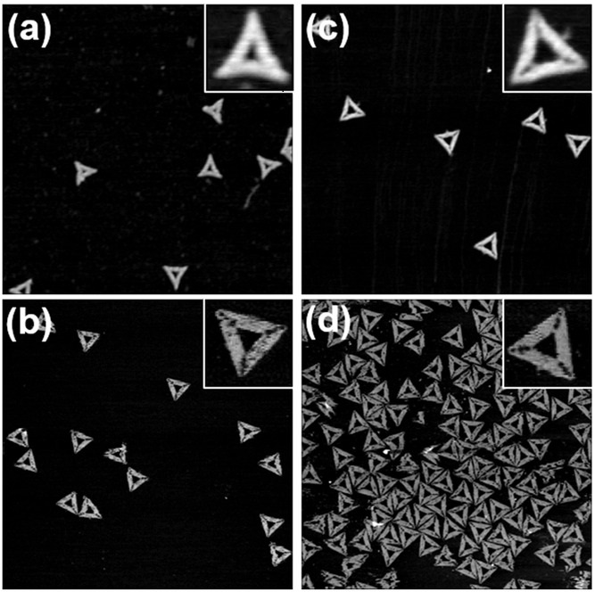
Effect of Staple Age on DNA Origami Nanostructure Assembly and Stability (https://www.nanoworld.com/blog/effect-of-staple-age-on-dna-origami-nanostructure-assembly-and-stability/?utm_source=Facebook&utm_medium=Blog&utm_content=Effect+of+Staple+Age+on+DNA+Origami+Nanostructure+Assembly+and+Stability&utm_campaign=NanoWorld+Blog) has been published on NanoWorld Blog. DNA origami nanostructures are widely employed in various areas of fundamental and applied research. Due to the tremendous success of the DNA origami technique in the academic field, considerable efforts currently aim at the translation of this technology from a laboratory setting to real-world applications, such as nanoelectronics, drug delivery, and biosensing. While many of these real-world applications rely on an intact DNA origami shape, they often also subject the DNA origami nanostructures to rather harsh and potentially damaging environmental and processing conditions.* In their article “Effect of Staple Age on DNA Origami Nanostructure Assembly and Stability” Charlotte Kielar, Yang Xin, Xiaodan Xu, Siqi Zhu, Nelli Gorin , Guido Grundmeier, Christin Möser, David M. Smith and Adrian Keller investigate the effect of long-term storage of the employed staple strands on DNA origami assembly and stability.* Atomic force microscopy (AFM) under liquid and dry conditions was employed to characterize the structural integrity of Rothemund triangles assembled from different staple sets that have been stored at −20 °C for up to 43 months.* NanoWorld Ultra-Short Cantilevers USC-F0.3-k0.3 were the AFM probes that were used for the AFM measurements under liquid conditions.* https://www.nanoworld.com/Ultra-Short-Cantilevers-USC-F0.3-k0.3.html Please have a look at the NanoWorld blog for the full citation and a direct link to the full article. #DNA #nanotechnology #AtomicForceMicroscopy

NANOSENSORS Nucleation in confinement generates long-range repulsion between rough calcite surfaces - news

Nucleation in confinement generates long-range repulsion between rough calcite surfacesMon Aug 05 2019

Nucleation in confinement generates long-range repulsion between rough calcite surfaces on NANOSENSORS™ Blog Fluid-induced alteration of rocks and mineral-based materials often starts at confined mineral interfaces where nm-thick water films can persist even at high overburden pressures and at low vapor pressures. These films enable transport of reactants and affect forces acting between mineral surfaces. However, the feedback between the surface forces and reactivity of confined solids is not fully understood.* In “Nucleation in confinement generates long-range repulsion between rough calcite surfaces» Joanna Dziadkowiec, Bahareh Zareeipolgardani, Dag Kristian Dysthe and Anja Røyne describe how they used the surface forces apparatus (SFA) to follow surface reactivity in confinement and measure nm-range forces between two rough calcite surfaces in NaCl, CaCl2, or MgCl2 solutions with ionic strength of 0.01, 0.1 or 1 M.* Roughness evolution with time of single, unconfined calcite films in salt solutions was analyzed by Atomic Force Microscopy using NANOSENSORS™ uniqprobe qp-SCONT AFM probes to image the surfaces in contact mode.* https://www.nanosensors.com/uniqprobe-uniform-quality-spm-probe-soft-contact-mode-qp-scont Please have a look at the NANOSENSORS™ blog for the full citation and a direct link to the full article. #AtomicForceMicroscopy #ChemicalPhysics #RoughnessCharacterization

NanoAndMore The Skeptics' Guide to the Universe - news

The Skeptics' Guide to the UniverseFri Aug 02 2019

Friction is everywhere — from a violinist bowing a string to children skidding down a slide. In the right situation, the ubiquitous force can have big effects: Interleave the pages of two phone books, and the friction between the pages will hold the books together so tightly that they become strong enough to suspend a car above the ground.

NanoWorld Happy Birthday Switzerland - news

Happy Birthday SwitzerlandThu Aug 01 2019

Happy Birthday Switzerland (https://www.nanoworld.com/blog/happy-birthday-switzerland/?utm_source=Facebook&utm_medium=Blog&utm_content=Happy+Birthday+Switzerland&utm_campaign=NanoWorld+Blog) has been published on NanoWorld Blog. It's the Swiss National Holiday today. Have fun everyone!

NANOSENSORS Happy Swiss National Holiday with Smallest Swiss Cross - news

Happy Swiss National Holiday with Smallest Swiss CrossWed Jul 31 2019

Happy Swiss National Holiday with Smallest Swiss Cross on NANOSENSORS™ Blog Basel University: Smallest Swiss Cross - Made of 20 Single Atoms ( a NANOSENSORS™ PPP-NCL was used for this image) 20 bromine atoms positioned on a sodium chloride surface using the tip of an atomic force microscope at room temperature, creating a Swiss cross with the size of 5.6nm. The structure is stable at room temperature and was achieved by exchanging chlorine with bromine atoms. (Fig: University of Basel, Department of Physics)

NanoWorld Ultra-high resolution imaging of thin films and single strands of polythiophene using atomic force microscopy - news

Ultra-high resolution imaging of thin films and single strands of polythiophene using atomic force microscopyMon Jul 29 2019

Ultra-high resolution imaging of thin films and single strands of polythiophene using atomic force microscopy (https://www.nanoworld.com/blog/ultra-high-resolution-imaging-of-thin-films-and-single-strands-of-polythiophene-using-atomic-force-microscopy/?utm_source=Facebook&utm_medium=Blog&utm_content=Ultra-high+resolution+imaging+of+thin+films+and+single+strands+of+polythiophene+using+atomic+force+microscopy&utm_campaign=NanoWorld+Blog) has been published on NanoWorld Blog. Real-space images of polymers with sub-molecular resolution could provide valuable insights into the relationship between morphology and functionality of polymer optoelectronic devices, but their acquisition is problematic due to perceived limitations in atomic force microscopy (AFM).* In the article “Ultra-high resolution imaging of thin films and single strands of polythiophene using atomic force microscopy” Vladimir V. Korolkov, Alex Summerfield, Alanna Murphy, David B. Amabilino, Kenji Watanabe, Takashi Taniguchi and Peter H. Beton show that individual thiophene units and the lattice of semicrystalline spin-coated films of polythiophenes (PTs) may be resolved using AFM under ambient conditions through the low-amplitude (≤ 1 nm) excitation of higher eigenmodes of a cantilever.* They authors demonstrate that the use of higher eigenmodes in tapping-mode ambient AFM can be successfully employed to characterize both individual polymer strands down to a single-atom level and also the ordering of a semi-crystalline polymer with technological relevance. The combination of AFM and solution deposition provides a simple and high-resolution approach to characterizing the structure of polymers.* The use of NanoWorld Arrow-UHF high frequency AFM probes at their first eigenmode of ~1.4 MHz is mentioned.* https://www.nanoworld.com/ultra-high-frequency-tapping-mode-afm-tip-arrow-uhf Please have a look at the NanoWorld blogpost for the full citation and a direct link to the full article. #AtomicForceMicroscopy #ImagingTechniques #MolecularSelfAssembly

BudgetSensors SEM image of CS-20NG AFN calibration nanogrid standard

BudgetSensors® HS or CS calibration grating!Mon Jul 22 2019

Get the most out of your BudgetSensors® HS or CS calibration grating! No surface is ideally smooth at the nanoscale, but that does not mean you cannot achieve highly accurate and precise calibration. Averaging the scan profile over several micrometers significantly improves your system's calibration. Check out our calibration gratings here: https://www.budgetsensors.com/calibration-standards 

NANOSENSORS Ferroelectricity-free lead halide perovskites – NANOSENSORS™ - news

Ferroelectricity-free lead halide perovskites – NANOSENSORS™Sun Jul 21 2019

Ferroelectricity-free lead halide perovskites on NANOSENSORS Blog. In the recent publication “Ferroelectricity-free lead halide perovskites” Andrés Gómez, Qiong Wang, Alejandro R. Goñi, Mariano Campoy-Quilesa and Antonio Abate describe how they employed direct piezoelectric force microscopy ( DPFM ) to examine whether or not lead halide perovskites exhibit ferroelectricity.* Their article aims to provide a deeper understanding of the fundamental physical properties of the organic–inorganic lead halide perovskites and solves a longstanding dispute about their non-ferroelectric character: an issue of high relevance for optoelectronic and photovoltaic applications.* In the course of their research in which besides using DPFM, they also employed piezoelectric force microscopy ( PFM ) and electrostatic force microscopy ( EFM ), they could demonstrate the non-ferroelectricity of lead halide perovskites. * The PFM images were acquired using a PtIr coated NANOSENSORS PPP-EFM AFM probe. https://www.nanosensors.com/PointProbe-Plus-Electrostatic-Force-Microscopy-PtIr5-Coating-afm-tip-PPP-EFM Please have a look at the NANOSENORS blog for the full citation and a direct link to the full article. #perovskite #photovoltaics #ElectrostaticForceMicroscopy #AFMprobes


Loading
nanosensors-logo
nanoworld-logo
budgetsensors-logo
mikromasch-logo
opus-logo
sqube-logo
nanotools-logo