discontinued 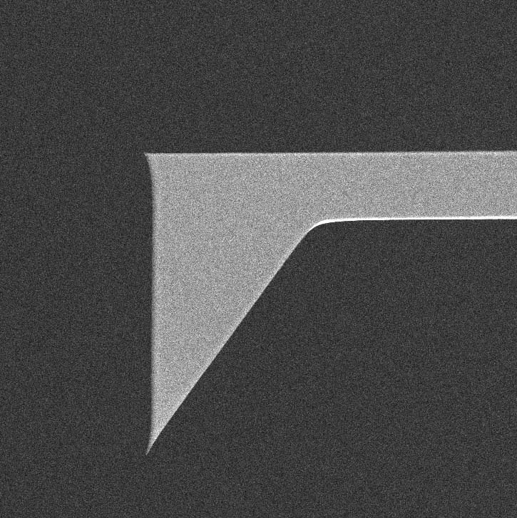 OLYMPUS**

How to find the OLYMPUS** replacement AFM probe that works for you:
Identify the order code of the discontinued OLYMPUS** AFM probe you have been using.
Click on the NanoAndMore replacement category showing the same order code.

Also known as OLYMPUS** AFM Probe TR800PSA (73kHz, 0.57N/m and 24kHz, 0.15N/m)
We offer different AFM tip shapes and several AFM probes brands to choose from, when replacing an OLYMPUS** AFM probe. Choose the option that suits your needs best.
If you need any explanation regarding the different AFM tip shapes that are available, please check the information below, called "About OLYMPUS** AFM Tips."
Request a free sample or place an online order. We will be happy to serve you!
OLYMPUS** Corp. has decided to stop producing their well-known AFM probes, also known as OLYMPUS** Micro Cantilevers, which have been on the market for decades. Over the last few years many of the well-known OLYMPUS** AFM probe types and series have been discontinued. In September 2022 Olympus Corporation declared the production end for the 5 remaining types of silicon-based OLYMPUS** AFM probes (https://www.olympus-global.com/products/)
Therefore, now all OLYMPUS** AFM probes are officially with status discontinued! Please refer to the OLYMPUS** website: https://www.olympus-global.com/products/
NanoAndMore has been receiving an influx of inquiries from concerned AFM users preparing to switch from the OLYMPUS** Probe to other AFM Probe brands to meet their specific AFM probe requirements
We have therefore prepared a detailed guide introducing the different possible options for alternatives.
In the following we will break down the different AFM tip shape types offered by NanoAndMore compared to the OLYMPUS** AFM tips shape.
Additionally, we also compare and highlight the variety of AFM probes brands offered by NanoAndMore:
from a mechanical-parameter point of view for each individual OLYMPUS** AFM probe type.
In order to enable an easy switch and to reduce a loss in time and frustration on the customer’s side, we are providing this information in dedicated subcategories here in this section.
There are two more points to mention before we get into comparing the different AFM tip shapes.
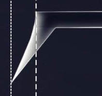
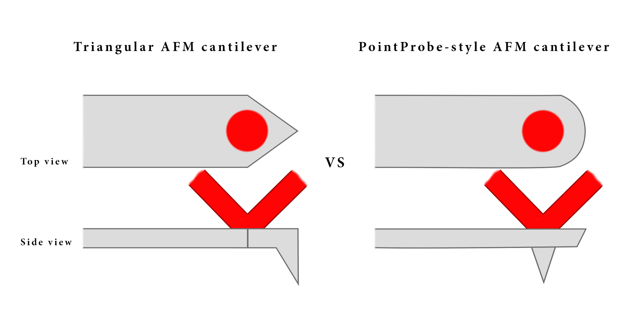 Fig.1: Lateral distance between laser spot and AFM tip for triangular and Pointprobe®-style AFM cantilevers
In general, the silicon-based OLYMPUS** AFM tip is a dry etched (around 90° sidewall) tetrahedral AFM tip at the end of the AFM cantilever. It has an AFM tip height of about 14um and an AFM tip radius of curvature of 7nm (specs taken from OLYMPUS** Microlever spec sheet).
 Fig.2: OLYMPUS** AFM tip shape side view
The main feature is that the AFM tip is positioned at the very end of the AFM cantilever. It allows for precise positioning of the AFM tip onto the point of interest on the sample. This is helpful for some applications and sample combinations. In this respect it must also be pointed out that once the AFM tip is mounted onto the AFM head under an angle of typically 12°–13°, the very end of the AFM tip is not visible anymore, but the feature of placing the AFM tip close to the point of interest remains.
Historically, the renowned, originally patented OLYMPUS** Micro Cantilever AFM probes were manufactured in-house at OLYMPUS** dedicated MEMS facility in Japan, utilizing SOI (Silicon-On-Insulator) wafers as the foundation of their design. This process, known for its precision and quality, remained in place for over two decades. However, around 2014, production was outsourced to an external MEMS foundry in Asia. In an effort to reduce costs and increase the number of AFM probe chips per wafer, the manufacturing approach was modified, shifting to a monolithic silicon wafer process. While the OLYMPUS** AFM tip and cantilever continue to be defined by a dry etch process, this transition introduced a fundamental change to the original OLYMPUS** AFM probe design and process philosophy.
The OPUS™ AFM tip is identical to the OLYMPUS** AFM tip in form, fit and function. The OPUS™ AFM tip as well as the OLYMPUS** AFM tip is a dry etched (around 90° sidewall) tetrahedral AFM tip at the end of the AFM cantilever with an AFM tip height of about 14um and a radius of curvature of 7nm.
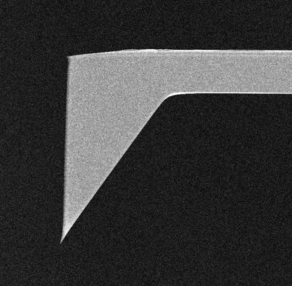

The OPUS™ AFM tip has been designed as a one-to-one replacement for the OLYMPUS** AFM tip and is therefore the perfect candidate in an upcoming replacement scenario for all silicon-based OLYMPUS** AFM probes.
Just like in the case of the OLYMPUS** style AFM tip the main feature of the OPUS™ AFM tip is that the AFM tip is positioned at the very end of the AFM cantilever, which helps the AFM user pointing the OPUS™ AFM tip onto the point of interest on the sample. Again, this is helpful for some applications and sample combinations. Same as for the OLYMPUS** AFM tip, it also must be pointed out that once the OPUS™ AFM tip is mounted onto the AFM head under an angle of typically 12°–13° the very end of the AFM tip is not visible anymore, but the feature of placing the AFM tip close to the point of interest remains.
OPUS™ AFM probes are made from SOI (Silicon-On-Insulator) wafers, with both the AFM tip and AFM cantilever precisely defined using a dry etch manufacturing process. OPUS™ therefore follows the original process design and philosophy pioneered by OLYMPUS**, ensuring high-quality and consistent probe performance without compromise.
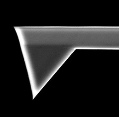
The AdvancedTEC™ AFM tip features a tetrahedral AFM tip that is different from the OLYMPUS** and OPUS™ style, because the AFM tip protrudes over the very end of the AFM cantilever. This very special feature allows precise positioning of the AFM tip onto the point of interest on the sample even once the AdvancedTec™ AFM probe is mounted onto the AFM head and tilted at 12° to 13° (see schematic below).
Since the AdvancedTEC™ AFM tip protrudes over the end of the AFM cantilever, it offers REAL TIP VISIBILITY FROM TOP and is the premium choice for all OLYMPUS** AFM probe users who have used OLYMPUS** AFM probes exactly for this specific feature of placing the AFM tip right onto the place of interest.


The AdvancedTEC™ AFM tip height is 15-20μm. The AFM tip radius of curvature is smaller than 10nm. The AdvancedTEC™ AFM probes series is produced from special monocrystalline highly doped silicon wafers.
Additionally, the AdvancedTEC™ AFM tip shape is defined by wet etching and therefore by real crystal planes that result in highly reproducible geometries and extremely smooth surfaces.
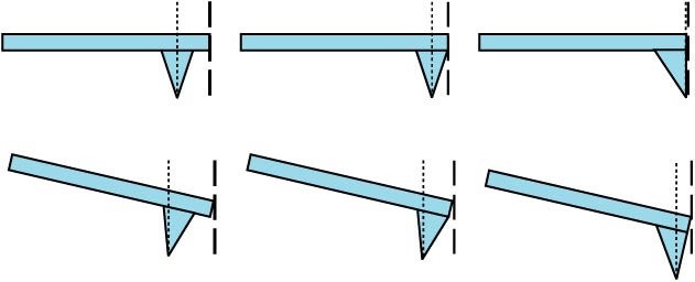
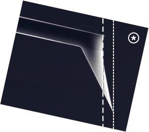
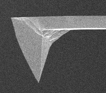
The Arrow AFM tip has a tetrahedral shape as the OLYMPUS** and OPUS™ AFM tips and it is located at the very end of the AFM cantilever. Contrary to the OLYMPUS** AFM tip and OPUS™ AFM tips, the Arrow AFM tip has no dry-etched 90° flank but a slightly inclined, wet-etched silicon plane (family silicon plane) that forms the very end of the Arrow AFM tip.


In addition to the fact that the AFM tip is at the very end and can be placed easily on the place of interest on the sample, the Arrow AFM tip offers the most symmetric scan in trace and retrace in X and Y direction for all silicon AFM tips once mounted tilted at 12°-13° onto the AFM head. This is due to the special sharpening of the Arrow AFM tip, which at the very end of the Arrow AFM tip results in a slight bend and tilts the very end of the AFM tip in the right direction, compensating the mounting angle (see schematic).
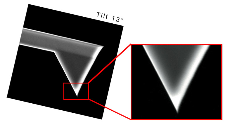
The Arrow AFM tip height is 10-15µm (3.5um for the Arrow UHF AFM probe type – high speed version) and the radius of curvature is typically <10nm. The AFM tip as well as the AFM cantilever is defined by wet-etching and features a very smooth and reproducible overall AFM tip shape. The Arrow AFM probes series is produced from special monocrystalline highly doped silicon wafers.


The standard polygon-based pyramid etched silicon AFM tip is, as the names suggests, shaped like a polygon-based pyramid. Its macroscopic half cone angle is 20° to 25° when viewed along the cantilever axis, 25° to 30° when viewed from the side and virtually zero at the very end of the AFM tip. This AFM tip style is fully wet-etched and features very smooth and reproducible surfaces.
In the following we also call this polygon-based pyramid etched AFM tip shape – Pointprobe® style because the NANOSENSORS™ Pointprobe® was the first commercially offered AFM tip of this style.
Contrary to the OLYMPUS**, OPUS™, Arrow and AdvancedTEC™ AFM tips, all polygon-based pyramid etched silicon AFM tips come with a tip setback (of about 15um) which means the AFM cantilever end is overhanging the tip position. This brings a slight disadvantage when it comes to precisely placing the AFM tip onto area of interest on the sample (please keep in mind the resolution limitation of your optical camera at the AFM setup!), however it shadows the deflection laser from the sample and helps to avoid the laser influencing the sample while performing the measurement in some applications and measuring modes.
Furthermore, for laser reflective coatings along with other back side coatings that should not reach and contaminate the AFM tip, the shadowing effect of the AFM cantilever of the Pointprobe® style AFM tip (tip setback) is essential during coating the back side of the AFM cantilever, because it prevents metal clusters and particles from depositing onto the AFM tip. This latter effect could result in an increased radius of curvature and/or other unwanted effects, and defects during the AFM measurement. An AFM tip at the end of the AFM cantilever at 90° or even more complicated - a protruding AFM tip end flank - can make the coating of only the back side of OLYMPUS**, OPUS™ and AdvancedTEC™ AFM cantilevers very difficult (not so for Arrow AFM tips as they offer the inclined, wet etched silicon AFM tip end).
The polygon-based pyramid etched silicon AFM tip is 10-15μm high (there are also tall versions available of up to 50um on the NANOSENSORS™ Special Developments List) and comes with radii starting with 2nm for super high-resolution imaging to standard radii of <7nm, <8nm, <10nm, … and radii of up to 200nm for nanomechanical measurements depending on the brand and/or AFM probe type, and model in question. Pointprobe® style AFM probes are produced on special monocrystalline highly doped silicon wafers.
Some brands (MikroMasch®, BudgetSenors®) offer a rotated PointPobe style AFM tip shape (meaning the Pointprobe® style AFM tip is rotated by 180° on the AFM cantilever) as standard and others (NANOSENSORS™, NanoWorld®) offer this as an option for some types and models.
In general, the Pointprobe® style AFM tip is by far the most versatile, AFM tip style worldwide. It comes in a wide variety of different AFM tip modifications, shapes and coatings – far too many to list here! Please contact us if you are looking for something out of the ordinary! We most likely have it available or have done it in the past and could have it reproduced on demand.
