High Aspect Ratio (HAR) AFM Probes
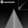
When an Atomic Force Microscope (AFM) probe is manufactured the formation of the AFM tip is done basically by etching a silicon crystal. When etching a crystal, the speed of the etch (the etch rate) is depending on the orientation of the crystal lattice. Depending on the initial state of the silicon wafer either a pyramidal tip is formed by underetching a masking pattern or a pyramidal pit is etched into the silicon which serves as the starting structure for molding the tip by a deposition of a silicon-nitride layer.
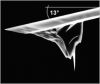
The resulting AFM tip pyramids have opening angles in between 50 and 70°. If now a surface is scanned with this AFM probe, the opening angle will affect the correct rendering of some sample features. As long as only flat samples are scanned no distortion by the AFM tip is visible in the image. But when imaging steeper features of a certain height the opening angle of the AFM tip pyramid will distort the scanning result. If a specimen has a vertical step, the aperture angle of the AFM tip pyramid will map it as an oblique step. Also, narrow trenches or holes could not be imaged correctly. This effect will occur at step heights of several hundred nanometers depending on the shape of the feature.
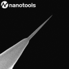
Most often, these kinds of distortions are acceptable and they are included in the interpretation of the AFM probe scanning image. But for certain groups of samples such as narrow gaps, trenches or holes, mostly in semiconductor manufacturing process control these falsifications are unacceptable. For such needs especially tailored AFM tips are manufactured: High Aspect Ratio AFM probes. This type of AFM probe features a needle-shaped AFM tip that should be perpendicular to the sample surface when imaging which can be achieved by compensating the mounting angle of the individual AFM instrument. Ideally it should also have the smallest possible diameter and parallel sidewalls.
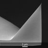
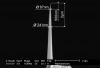
High Aspect Ratio AFM probes can be manufactured using two different approaches: The first approach is to further refine the tip apex of the silicon AFM tip. A needle is carved out of the silicon pyramid. With a so-called Focussed Ion Beam (FIB) milling process silicon atoms are removed by sputtering. A very narrow beam of gallium atoms is accelerated onto the AFM tip apex. When they hit the surface, they are knocking silicon atoms out of the AFM tip pyramid. With a skillful control of the incident beam of gallium atoms a needle-shaped structure can be worked out. Nevertheless, this technology has some disadvantages. It is not possible to create perfect cylinders with parallel side walls, but a slight cone shape always occurs. Also, the smallest diameter that can be achieved is limited. But as long as the structure to be measured is not smaller than a few hundred nanometers, this kind of AFM probe works well.
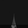
If smallest structures and holes need to be imaged, where High Aspect Ratio AFM tips manufactured by Focussed Ion Beam (FIB) are not suitable anymore, needles with the smallest possible diameters and perfectly parallel sidewalls are essential. High Aspect Ratio AFM probes made from highly dense carbon are then the AFM probe of choice. With the so-called Electron Beam Deposition (EBD) technology an extra AFM tip at the apex of the silicon AFM tip pyramid is grown. Carbon gas is introduced into a vacuum where the AFM tip is located. A well-defined electron beam locally activates the surface and carbon atoms will agglomerate. By this method simple geometries out of diamond-like-carbon could be generated. To create a High Aspect Ratio AFM tip, a thin cylinder is grown. With this technique, extremely thin needles with diameters down to 10 nanometers or lengths up to several micrometers can be fabricated. These carbon extra-AFM tips have an extraordinary diamond-like hardness. The range of dimensions for the high aspect ratio portion of those AFM probe could vary from 10nm in diameter and 100nm in length up to lengths of about 8 microns.
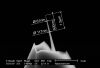
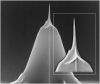
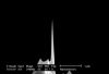
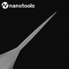
AR10T Close-up 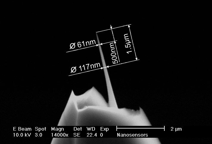
Close-up SEM image of a NANOSENSORS™ AR10T High Aspect Ratio AFM probe, manufactured by Focussed Ion Beam (FIB) milling.
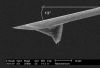
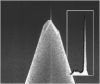
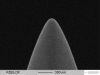
M1-HAR Close-up 
Silicon AFM tip pyramide with a high-density carbon spike, manufactured by Electron Beam Deposition (EBD).
Ordinary AFM tips are usually manufactured in full wafers of several hundred AFM chips at one time. Speciality AFM probes such as High Aspect Ratio AFM probes, on the other hand have to be manufactured in a single AFM tip production process which leads to a comparatively higher price.
Some applications like very narrow features with a high aspect ratio, such as very small and shallow holes, are better imaged with a high resolution AFM probe, which has an even better aspect ratio than High Aspect Ratio AFM tip at the very end of the AFM tip apex.
Sort by:
19 results
best of the best

AR10T-NCHR
High-Aspect-Ratio, Tilt Compensated Tapping Mode AFM Probe
Coating:
Reflective Aluminum
Tip Shape: High-Aspect-Ratio
Tip Shape: High-Aspect-Ratio
AFM Cantilever:
F
330 kHz
C
42 N/m
L
125 µm
AR5T-NCHR
High-Aspect-Ratio, Tilt Compensated Tapping Mode AFM Probe
Coating:
Reflective Aluminum
Tip Shape: High-Aspect-Ratio
Tip Shape: High-Aspect-Ratio
AFM Cantilever:
F
330 kHz
C
42 N/m
L
125 µm
the industry standard

NW-AR5T-NCHR
High-Aspect-Ratio, Tilt Compensated Tapping Mode AFM Probe
Coating:
Reflective Aluminum
Tip Shape: High-Aspect-Ratio
Tip Shape: High-Aspect-Ratio
AFM Cantilever:
F
330 kHz
C
42 N/m
L
125 µm
TESPA-HAR
High-Aspect-Ratio, Tapping Mode AFM Probe
Coating:
Reflective Aluminum
Tip Shape: High-Aspect-Ratio
Tip Shape: High-Aspect-Ratio
AFM Cantilever:
F
320 kHz
C
42 N/m
L
125 µm
top value

160AC-FG
High Aspect Ratio, Tapping Mode AFM Probe with AFM Tip at the Very End of the AFM Cantilever
Coating:
Reflective Gold
Tip Shape: High-Aspect-Ratio
Tip Shape: High-Aspect-Ratio
AFM Cantilever:
F
300 kHz
C
26 N/m
L
160 µm
New
240AC-FG
High Aspect Ratio, Force Modulation AFM Probe with AFM Tip at the Very End of the AFM Cantilever
Coating:
Reflective Gold
Tip Shape: High-Aspect-Ratio
Tip Shape: High-Aspect-Ratio
AFM Cantilever:
F
70 kHz
C
2 N/m
L
240 µm

EBD-AR15T
High-aspect ratio, tilt compensated EBD AFM whisker for automated non-contact AFM
Coating:
none
Tip Shape: High-Aspect-Ratio,Cone Shaped,EBD
Tip Shape: High-Aspect-Ratio,Cone Shaped,EBD
AFM Cantilever:
F
330 kHz
C
40 N/m
L
125 µm
AR10-NCHR
High-Aspect-Ratio, Tapping Mode AFM Probe
Coating:
Reflective Aluminum
Tip Shape: High-Aspect-Ratio
Tip Shape: High-Aspect-Ratio
AFM Cantilever:
F
330 kHz
C
42 N/m
L
125 µm
AR5-NCHR
High-Aspect-Ratio, Tapping Mode AFM Probe
Coating:
Reflective Aluminum
Tip Shape: High-Aspect-Ratio
Tip Shape: High-Aspect-Ratio
AFM Cantilever:
F
330 kHz
C
42 N/m
L
125 µm
AR5-NCH
High-Aspect-Ratio, Tapping Mode AFM Probe
Coating:
none
Tip Shape: High-Aspect-Ratio
Tip Shape: High-Aspect-Ratio
AFM Cantilever:
F
330 kHz
C
42 N/m
L
125 µm
NW-AR10-NCHR
High-Aspect-Ratio, Tapping Mode AFM Probe
Coating:
Reflective Aluminum
Tip Shape: High-Aspect-Ratio
Tip Shape: High-Aspect-Ratio
AFM Cantilever:
F
320 kHz
C
42 N/m
L
125 µm
NW-AR5-NCHR
High-Aspect-Ratio, Tapping Mode AFM Probe
Coating:
Reflective Aluminum
Tip Shape: High-Aspect-Ratio
Tip Shape: High-Aspect-Ratio
AFM Cantilever:
F
320 kHz
C
42 N/m
L
125 µm
AR5-NCLR
High-Aspect-Ratio, Tapping Mode AFM Probe with Long AFM Cantilever
Coating:
Reflective Aluminum
Tip Shape: High-Aspect-Ratio
Tip Shape: High-Aspect-Ratio
AFM Cantilever:
F
190 kHz
C
48 N/m
L
225 µm
NW-AR5-NCLR
High-Aspect-Ratio, Tapping Mode AFM Probe with Long Cantilever
Coating:
Reflective Aluminum
Tip Shape: High-Aspect-Ratio
Tip Shape: High-Aspect-Ratio
AFM Cantilever:
F
190 kHz
C
48 N/m
L
225 µm
M-CIS
EBD AFM whisker for non-contact AFM microlens contact image sensor (CIS) inspection
Coating:
Reflective Aluminum
Tip Shape: High-Aspect-Ratio,Cone Shaped,EBD
Tip Shape: High-Aspect-Ratio,Cone Shaped,EBD
AFM Cantilever:
F
320 kHz
C
40 N/m
L
120 µm
EBD-HAR
Universal high-aspect ratio EBD AFM whisker for enhanced resolution, imaging stability and AFM tip lifetime
Coating:
none
Tip Shape: High-Aspect-Ratio,Cone Shaped,EBD
Tip Shape: High-Aspect-Ratio,Cone Shaped,EBD
AFM Cantilever:
F
330 kHz
C
40 N/m
L
125 µm
EBD-AR20T
High-aspect ratio, tilt compensated EBD AFM whisker for automated non-contact AFM
Coating:
none
Tip Shape: High-Aspect-Ratio,Cone Shaped,EBD
Tip Shape: High-Aspect-Ratio,Cone Shaped,EBD
AFM Cantilever:
F
330 kHz
C
40 N/m
L
125 µm
M1-HAR
High-aspect ratio, tilt compensated EBD AFM whisker for automated non-contact AFM
Coating:
none
Tip Shape: High-Aspect-Ratio,Cone Shaped,EBD
Tip Shape: High-Aspect-Ratio,Cone Shaped,EBD
AFM Cantilever:
F
320 kHz
C
40 N/m
L
120 µm
NANOSENSORS™ Special Developments List (SDL)
Special AFM Probes etc. Showcasing NANOSENSORS™ Expertise
Coating:
various
Tip Shape: various
Tip Shape: various