AFM Probe Fabrication

AFM probe fabrication

This note is a brief guide to silicon AFM probe fabrication. It is intended for those who want to learn about how AFM probes are produced and have little or no experience in the field of semiconductor technology.


General Micro-Patterning Process

Silicon AFM probes are fabricated on single crystal silicon wafers. The wafers are patterned in a micromachining process in order to obtain the desired structures. The general step sequence for one structuring step is shown below.


1. Blanket silicon waferIt is important to start with a high-quality monocrystalline silicon wafer with few defects and a smooth, clean surface.
Blanket_silicon_wafer
2. Hardmask layer deposition / growthPhotoresist is not resistant against silicon-etching chemicals such as potassium hydroxide (KOH). This is why an additional layer of silicon oxide or silicon nitride is deposited or grown on the silicon surface as a protective 'hardmask' during the silicon etch.
Hardmask layer deposition / growth
3. Photoresist depositionThe wafer is coated with a photosensitive film (photoresist) and then baked in order to harden it. A positive photoresist, like the one used in our example, becomes soluble in photoresist developer after exposure to ultraviolet light. Negative photoresists, which become insoluble after UV exposure, are also available.
Photoresist deposition
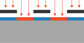
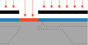
4. ExpositionAn optical mask with a certain structure pattern is positioned over the wafer and then the wafer is exposed to ultraviolet light. The light softens the exposed photoresist areas.
Exposition
5. Photoresist developmentThe photoresist in the developed areas is dissolved in a photoresist developer, exposing the hardmask layer. The photoresist is baked again to harden it further.
Photoresist development
6. Oxide / nitride hardmask patterningThe photoresist pattern is transferred to the hardmask layer by etching in acid, typically hydrofluoric acid (HF) for silicon oxide and phosphoric acid (H3PO4) for silicon nitride.
Oxide / nitride hardmask patterning
7. Photoresist removalThe remaining photoresist is stripped from the wafer in acetone.
Photoresist removal
8. Substrate patterningThe pattern is transferred to the silicon substrate by a KOH etch.
Substrate patterning
9. Oxide / nitride removalFinally the mask layer is removed, leaving the structured silicon surface.
Oxide / nitride removal

Photolithography is the general term for the technique of transferring geometric patterns from the mask to the photoresist covering the substrate surface. It includes the photoresist deposition, baking, exposition, development and stripping, as well as the related cleaning steps. Broader definitions include the thin film or substrate etching steps as well.
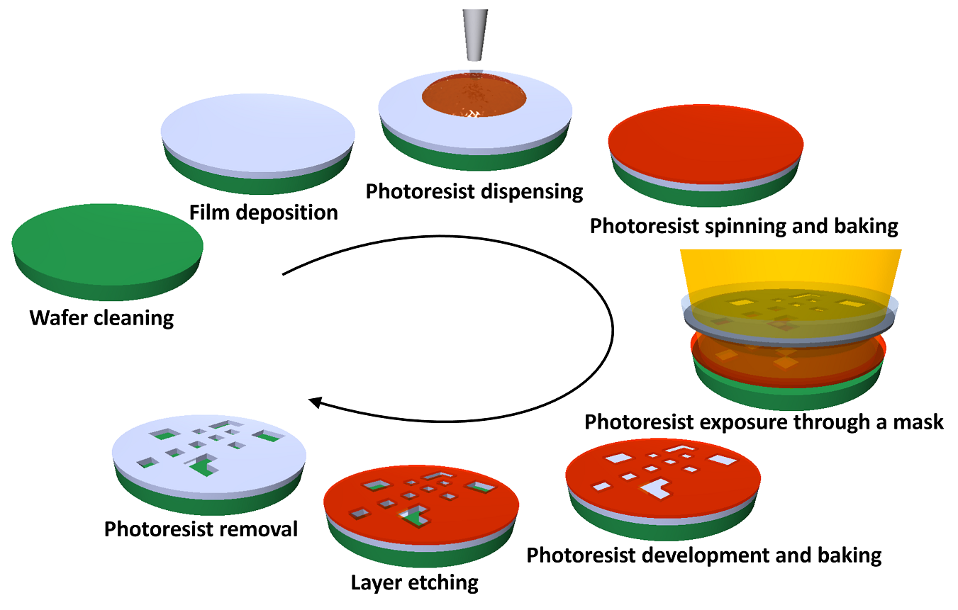
3D schematics of the photolithography and layer etching steps

The photolithography mask features a repeatable pattern which allows transferring simultaneously a large number of identical structures on to the wafer. This makes the process much more efficient than single unit production. Usually, several hundred AFM probes are produced on a wafer.

Various cleaning steps are performed at different stages of processing. They are of immense importance to the fabrication process. Cleaning removes residual particles and chemicals from the wafer surface. As a result, defect density decreases significantly, while photoresist and layer adhesion improve significantly, both of which increase the yield.

Yield is very important in the world of microfabrication. In order to achieve high overall yields, the yields of individual steps must be orders of magnitude higher. Therefore, every single processing step must be carried out with great care and under strict control over process parameters.


General AFM Probe Fabrication Steps

The AFM probe fabrication processes vary for different AFM probe types and for different manufacturers. Different technological processes, process parameters and step sequences are applied. They have a significant impact on the final product quality and yield.

The process flow described below is a simplified version of an actual fabrication process, which consists of over 100 steps and takes a couple of months to complete.

1. Blanket silicon wafer AFM probe fabrication starts with a blanket monocrystalline silicon wafer with crystallographic orientation (100).
1.Blanket_silicon_wafer
2. Oxidation A thick oxide is grown on both sides of the silicon wafer.
2.Oxidation
3. Chip photolithography, oxide etch and silicon etch (bottom side) The first photolithography is performed on the back of the wafer using the chip mask. After oxide etch, the silicon substrate is patterned by potassium hydroxide (KOH) etch.
3.Chip_photolithography_oxide_etch_and_silicon_etch_bottom_side
4. AFM cantilever photolithography, oxide etch and silicon etch (top side) The second patterning step defines the lateral dimensions of the AFM cantilevers. The silicon etch determines their thickness.
4.Cantilever_photolithography_oxide_etch_and_silicon_etch_top_side
5. AFM tip photolithography, oxide etch and silicon etch (top side) The third and final photolithography defines the AFM tip geometry.
5.AFM_tip_photolithography_oxide_etch_and_silicon_etch_top_side
6. Oxide removal (top side) The remaining oxide on the top side of the wafer is removed in order to provide a clean surface for the next oxidation.
6.Oxide_removal_top_side
7. Oxidation and protective nitride deposition (top side) An additional silicon nitride layer is deposited on top of a thin oxide layer in order to serve as a protective layer for the next step.
7.Oxidation_and_protective_nitride_deposition_top_side
8. Chip-release silicon etch (bottom side) The last silicon etch step releases the AFM cantilever and the chip from the rest of the silicon substrate.
8. Chip release silicon etch (bottom side)
9. Nitride and oxide removal, wafer complete After the nitride and oxide layer are removed, the AFM probes are separate units loosely held to the wafer frame and the AFM probe fabrication is complete.
9._Nitride_and_oxide_removal

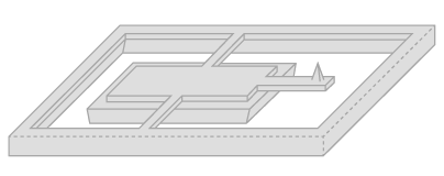
The finished silicon wafer contains several hundred AFM probes. The AFM probes are attached to the wafer only by two small silicon bridges on each side of the holder chip. The AFM probes can be easily freed by applying a small mechanical force to the holder chip with tweezers.
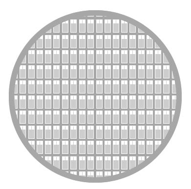
Wafer with AFM Probes
One wafer cell with AFM probe and bridges holding it to the frame
Loading
nanosensors-logo
nanoworld-logo
budgetsensors-logo
mikromasch-logo
opus-logo
nanotools-logo