The Nano eNabler molecular printing system includes: the printer (Nano eNabler™), the print cartridges (SPT™) and the “paper” (Sindex™ Chips)
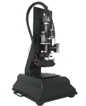
The Nano eNabler System™ at the right embodies proprietary instrumentation and methodology for creating a broad spectrum of new nanotechnology applications.
This device places molecules at defined locations on a surface with nanometer spatial resolution. The arrays of molecules are unique to BioForce and can only be created with a Nano eNabler System™.
The Nano eNabler System™ prints proteins and other biological and non-biological materials onto silicon chips and other surfaces with ultra-micro spot sizes ranging from 20 microns to 1 micron, and in the nanometer range to 250 nm.
Ultramicro- or nanoarrays of up to 10-50 domains or more can readily be produced and can subsequently be used as ultraminiature test sites for biomolecular interactions.
An SPT™ (Surface Patterning Tool) is the molecular “ink cartridge” for our desktop molecular printer (Nano eNabler™).

Each SPT is a microcantilever-based micro-fluidic handling device. SPTs contain either a single microcantilever print head or multiple microcantilevers for simultaneous printing of multiple molecular species. The integrated microfluidic network transports fluid samples from reservoirs located on the SPT through microchannels to the distal end of the cantilever.
Thus SPTs can be used to print materials that include biological samples such as proteins, DNA, RNA, and whole viruses, as well as non-biological samples such as chemical solutions, colloids and particle suspensions.
BioForce Nanosciences Inc. supplies a variety of different SPTs to meet a broad range of customer needs and can also provide custom SPT design and fabrication.
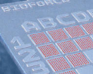
The Sindex™ Chips provide ideal printing surfaces for the desktop molecular printer (Nano eNabler™).
These 4x4 mm silicon substrates contain topographically defined pads that are arrayed within an alphanumeric indexing system. The pads are flat and smooth, making them compatible with conventional (e.g., fluorescence) and nonconventional (e.g., atomic force microscopy) readout mechanisms.
The indexing system allows precise location and relocation of specific positions on the chip. The surface can be coated with different metals and treated by a variety of approaches to render it chemically reactive.
The Nano eNabler™ benchtop molecular printer is a new and enabling technology for ultramicro- and nanoscale fluid delivery. It is a versatile platform capable of delivering attoliter to femtoliter (10-18 to 10-15 liter) volumes of solutions containing biomolecules and other materials to defined locations on surfaces with 1 to 20 μm feature sizes and nanometer spatial resolution.
The Nano eNabler™ benchtop molecular printer’s unique features offer:
We’ve heard from our users about several very important benefits they appreciate, including:
| Material Deposited | Representative Applications |
| Antibodies and other proteins | Biosensors, biomedical devices, molecular screening, cell biology, nanobiology |
| Nucleic acids | Gene chips, genomics, biosensors |
| Viruses | Biosensors, diagnostics, nanodevices |
| Adhesives | MEMS, nanodevices |
| Colloidal particles | Electronics, nanodevices, materials R&D |
| Quantum dots | Optical devices, diagnostics, materials R&D |
| Etchants, solvents, catalysts | MEMS, electronics, microfabrication |
The Nano eNabler™ System is a multifaceted tool for printing and manipulating materials at the ultra-micro and nanoscales. Just a few of the applications include:
- Biosensors: Placement of biomaterials on sensor platforms.
- Biomarker screening: Creation of multiplexed biomarker arrays that require minimal sample (a few or even single cells).
- Ultramicro and nanoscale device construction: Precise mechanical placement of materials in defined patterns to seed and/or create novel nanostructures.
- DNA manipulation: Deposition and manipulation of large DNA molecules.
- Sample preparation for AFM: Placement of materials in areas sufficiently small to permit analysis by atomic force microscopy.