PeakForce Tapping™ AFM Probes
In 2000 an advancement of the omnipresent Tapping Mode was made by WiTEC, by inventing the so-called Pulsed Force Mode. In Tapping mode the AFM cantilever oscillates close to its resonance frequency in a well-defined height above the sample in such a way, that in the lower reversal point of the oscillation the interaction regime changes from attractive to repulsive forces. Colloquially said, the surface is slightly touched (tapped) by the AFM tip.
Changes in samples topography implicate changes in the tip-sample-interaction. Those are detected either by a change of the amplitude or the phase of the AFM cantilever oscillation. Even if the interaction time is extremely short, the AFM cantilever taps with its resonance frequency some hundred thousand times per second to the sample surface. Even with a fast feedback loop it will take many taps of the tip onto the surface until the pre-chosen interaction force is reset again.
In Pulsed Force Mode the AFM cantilever is not oscillated at its resonance anymore, but at a fixed frequency, and every single oscillation of the AFM tip is analyzed. Thus, tip-sample-interaction could be well adjusted and minimized.
Pulsed Force Mode was taken up by Bruker and implemented into their AFMs as the so called PeakForce Tapping™** Mode. PeakForce Tapping™** is an off-resonance mode in which the AFM cantilever oscillations are performed at a rate much lower than the natural resonance frequency of the AFM cantilever. Beside the standard topography information, each AFM cantilever oscillation is regarded as a single force curve. Analyzing those curves allows to adjust and minimize interaction forces down to some hundred piconewtons and lead to information about the sample mechanical properties as like as adhesion, stiffness or viscosity.
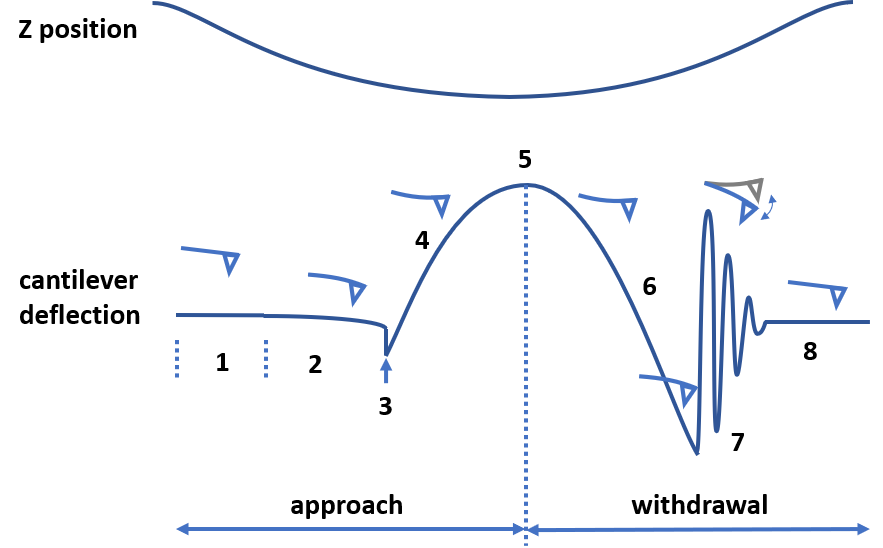
Fig. 1. Z piezo position and AFM cantilever deflection during a PeakForce tapping™** cycle with (1) baseline, (2) van der Waals attraction, (3) snap into contact, (4) deflection / indentation (5) ‘peak’ force (6) retraction (7) ringing / resonance oscillation and (8) baseline.
The schematic illustrates one PeakForce Tapping™** force-curve cycle. As the piezo gradually extends towards the sample and then retracts from it, the cycle passes through the following points:
1. Baseline. AFM cantilever is far from the surface, no AFM cantilever deflection
2. Long-range van der Waals forces deflect the AFM cantilever slightly towards the surface
3. The AFM tip snaps into contact with the surface
4. The AFM probe is pressed into the surface and the AFM cantilever deflects in the opposite direction. away from the surface
5. Point of maximum or ‘peak’ force is reached. (used to control the interaction and obtain he topography)
6. The AFM probe is retracted from the surface. AFM cantilever deflection decreases, passes through zero and then the AFM cantilever sticks to the surface and is deflected towards the surface again due to adhesion forces.
7. By further retracting the AFM cantilever from the surface, the AFM tip breaks-off from the surface. The AFM cantilever ‘rings’ i.e. oscillates at its natural resonance frequency for a while.
8. Baseline. Ideally the oscillation should be sufficiently attenuated before the next cycle starts so that an accurate baseline can be obtained.
By determining a) calibrate photodetector to AFM cantilever deflection (deflection sensitivity) and b) AFM cantilever force constant, the photodetector output in volts is converted to force and quantitative force measurements can be achieved.
By converting the cantilever deflection within the photo detector signal (deflection sensitivity) and determining the force constant of the cantilever by a thermal tune measurement, the tip-sample-interaction can be displayed directly as a quantifiable force. Tip-sample interactions can be minimized to ensure low tip wear and force curves can be analyzed towards sample materials property.
The maximum or ‘peak’ force in each cycle is used as a trigger for the piezo to retract, hence the name PeakForce Tapping™**. As direct control of the interaction force is achieved, low forces of around a few Nanonewtons, far less than used in Tapping Mode can be applied, leading to low AFM tip and sample damage with consistent imaging at high resolution for a wide range of materials from hard metals and ceramics to delicate bio samples such as DNA and other bio samples in liquids.
Quantitative nanomechanical information about adhesion, modulus, deformation and energy dissipation is inherently contained in and can be extracted directly from the PeakForce Tapping™** force-distance curves.
PeakForce Tapping™** also enables novel electrical and electrochemical property measurement modes such as PeakForce TUNA™** (PF-TUNA), PeakForce Kelvin probe force microscopy (PF-KPFM) and PeakForce scanning electrochemical microscopy (PF-SECM).
Bruker’s ScanAsyst mode for continuous and automated scan parameter self-optimization for image quality control is based on PeakForce Tapping™** mode.
In addition to the AFM probes listed below, you can also consider the NANOSENSORS™ Special Developments List AFM probes SD-R30-NCH and SD-R30-FM (R=30nm), and the SD-T7L100 (C=600N/m).
Sort by:
40 results