

BudgetSensors® ContDLC AFM Probes used in a recent studyMon Jun 13 2022
Friction force measurements with our diamond-like carbon coated ContDLC AFM probes reveal multiple symmetries for frictional anisotropy of atomic scale ripples in molybdenum disulfide

Studying MOCVD deposition of MoTe2 thin films on 8-inch SiO2/Si substratesThu Jun 09 2022
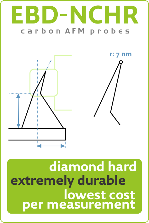
Discover how nanotools EBD-NCH with consistent radius are applied for characterizing growth, morphology, and thickness of MoTe2 thin films.
- Title: Wafer-Scale Epitaxial 1T′, 1T′–2H Mixed, and 2H Phases MoTe2 Thin Films Grown by Metal–Organic Chemical Vapor Deposition
DOI: 10.1002/admi.201800439 - Authors: TaeWan Kim, Hyeji Park, DaeHwa Joung, et al
- Publication: Advanced Materials Interfaces
- Publisher: John Wiley and Sons
- Date: Jun 4, 2018


Adsorption of SARS-CoV-2 Spike Protein S1 at Oxide Surfaces Studied by High-Speed Atomic Force MicroscopyWed Jun 08 2022
The ongoing coronavirus disease 2019 (COVID-19) pandemic caused by the severe acute respiratory syndrome coronavirus 2 (SARS-CoV-2) represents a serious threat to the health of millions of people. Respiratory viruses such as SARS-CoV-2 can be transmitted via airborne and fomite routes. The latter requires virion adsorption at abiotic surfaces and most likely involves the SARS-CoV-2 spike protein subunit 1 (S1), which is the outermost point of its envelope. Understanding S1 spike protein interaction with fomite surfaces thus represents an important milestone on the road to fighting the spread of COVID-19.*
In the article “Adsorption of SARS-CoV-2 Spike Protein S1 at Oxide Surfaces Studied by High-Speed Atomic Force Microscopy “ Yang Xin, Guido Grundmeier and Adrian Keller describe how high-speed atomic force microscopy (HS-AFM) is used to monitor the adsorption of the SARS-CoV-2 spike protein S1 at Al2O3(0001) and TiO2(100) surfaces in situ. *
Please have a look at the NanoWorld blog for the full citation and a direct link to the full article.
#CoronavirusSpikeProtein #molecularbiology #videorateAFM #高速AFMプローブ #高速原子力显微镜 #AFMprobes
#CoronavirusSpikeProtein #molecularbiology #videorateAFM #高速AFMプローブ #高速原子力显微镜 #AFMprobes
NanoWorld Ultra-Short Cantilevers of the USC-F0.3-k0.3 AFM probe type were used for the high-speed atomic force microscopy. *

")
Today we remember the late Heinrich Rohrer.Mon Jun 06 2022
The Swiss physicist - Heinrich Rohrer, born on this date in 1933, shared half of the 1986 Nobel Prize in Physics with Gerd Binnig (on the right) for the invention of the Scanning Tunneling Microscope (STM), the daddy of the Atomic Force Microscope (AFM). Thank you for leading the way!

Novel characteristics of soluble fibrin: hypercoagulability and acceleration of blood sedimentation rate mediated by its generation of erythrocyte-linked fibersSat Jun 04 2022
Soluble fibrin (SF) in blood consists of monomers lacking both fibrinopeptides A with a minor population in multimeric clusters. It is a substantial component of isolated fibrinogen (fg), which spontaneously self-assembles into protofibrils progressing to fibers at sub-physiologic temperatures, a process enhanced by adsorption to hydrophobic and some metal surfaces.
Read more...

Modified MikroMasch® HQ:CSC37/No Al AFM Probes with increased AFM tip radius have been used for the friction measurements.Fri May 27 2022
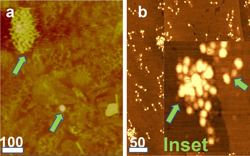
Exciting new research on the effects of roughness in dry and aqueous environment on the velocity dependence of friction in calcite crystals with implications for understanding and predicting seismicity. Modified MikroMasch HQ:CSC37/No Al AFM probes with increased AFM tip radius have been used for the friction measurements.
Influence of B/N co-doping on electrical and photoluminescence properties of CVD grown homoepitaxial diamond filmsWed May 25 2022
Boron doped diamond (BDD) has great potential in electrical, and electrochemical sensing applications. The growth parameters, substrates, and synthesis method play a vital role in the preparation of semiconducting BDD to metallic BDD. Doping of other elements along with boron (B) into diamond demonstrated improved efficacy of B doping and exceptional properties.
Read more...
AFM with large and ultrasharp tips is used to explore arterial tissue stiffness at two scalesTue May 17 2022
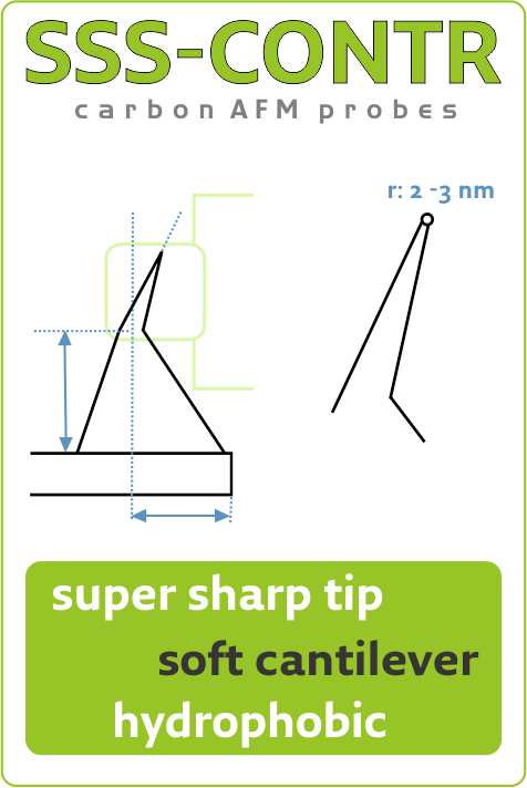
Discover how nanotools SuperSharpStandard-CONTR with 2-3 nm radius and biosphere™ with 2 µm and 5 µm radius are applied for soft tissue indentation measurements.
- Title: Revealing Layer-Specific Ultrastructure and Nanomechanics of Fibrillar Collagen in Human Aorta via Atomic Force Microscopy Testing: Implications on Tissue Mechanics at Macroscopic Scale
DOI: 10.1002/anbr.202100159 - Authors: Meisam Asgari, Neda Latifi, Francesco Giovanniello, Horacio D. Espinosa, Marco Amabili
- Publication: Advanced NanoBiomed Research
- Publisher: Wiley Online Library
- Date: 10 February 2022
https://nanotools.com/blog/afm-with-large-and-ultrasharp-tips-is-used-to-explore-arterial-tissue-stiffness-at-two-scales.html
#AFM #metrology #topography #microscopy #nanotechnology

Happy birthday, Prof. Christoph Gerber!Sun May 15 2022
Happy 80th anniversary to the Swiss professor Christoph Gerber, co-inventor of the Atomic Force Microscope!

BudgetSensors® new post!Wed May 11 2022
“The first principle is that you must not fool yourself and you are the easiest person to fool.” - theoretical physicist, Nobel price laureate and great popularizer of physics Richard Feynman, May 11, 1918 – February 15, 1988

Piezoelectricity of green carp scalesThu May 05 2022
Today is Children’s Day in Japan and many mulit-colored carp-shaped koinobori streamers are fluttering in the wind.
So it is the perfect day to repost and share the publication “Piezoelectricity of green carp scales” by Y. Jiang et al. with you.
Read about it on NanoWorld® Blog

MikroMasch® HQ:NSC18/Pt used in a recent studyMon May 02 2022
An improved approach to Conductive AFM based Electrical Contact Resistance measurements is developed and tested with the help of our MikroMasch® HQ:NSC18/Pt.
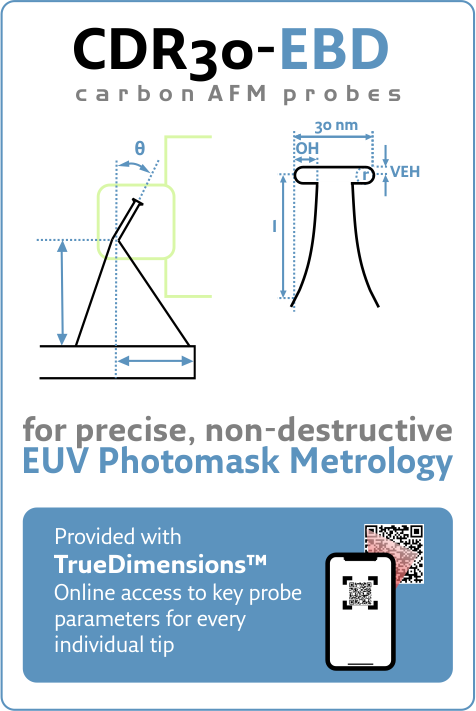
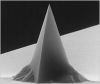
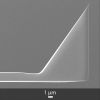
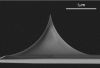
German National Metrology Institute (PTB) Scientists study CD-AFM and TEM for reference EUV Photomask MetrologyWed Apr 13 2022
Discover how nanotools CDR30-EBD with precisely controlled 30 nm width is applied to measure nanostructures of EUV photomask standards.
- Title: Comparison of EUV Photomask Metrology Between CD‑AFM and TEM
DOI: 10.1007/s41871-022-00124-y - Authors: Gaoliang Dai, Kai Hahm, Lipfert Sebastian and Markus Heidelmann
- Publication: Nanomanufacturing and Metrology
- Publisher: Springer Nature
- Date: February 3, 2022

BudgetSensors® ElectriTap300-G platinum coated AFM probes used in a recentWed Apr 06 2022
Silicon carbide stacking-order-induced doping variation in epitaxial graphene is analyzed with KPFM measurements using our ElectriTap300-G platinum coated AFM probes.
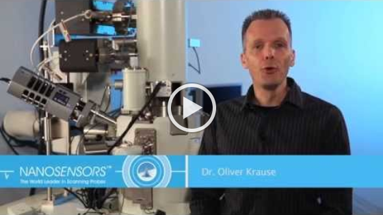
AFM probes for high resolution imaging – NANOSENSORS™ SuperSharpSilicon™ series video reaches 500 views markMon Apr 04 2022
The NANOSENSORS™ screencast on SuperSharpSilicon™ AFM probes for high resolution imaging held by Dr. Oliver Krause just passed the 500 views mark. Congratulations Oliver!
Read more...

Carbon dating in the AFM tip worldFri Apr 01 2022
Have you every wondered how carbon dating in the AFM tip world works?


MikroMasch® DLC coated AFM Probes HQ:NSC14/Hard/Al_BS AFM used in a recent studyMon Mar 21 2022
Our DLC coated HQ:NSC14/Hard/Al_BS AFM probes assist pressure-induced generation of lubricious interfacial layers of ionic liquid on steel surfaces.
biosphere™: Now available with 5 micron radiusWed Mar 16 2022
Green Line product update:
biosphere™: new 5 µm sphere radius on your preferred cantilever upon request
- Controlled tip radius: precisely fabricated spherical tips available with 12 different radii from 20 nm - 2 µm + now also with 5 µm.
- Pre-calibrated cantilevers: individually pre-calibrated cantilever spring constant using Laser Doppler Vibrometer.
Standard with 40, 2.8, and 0.2 N/m (other k available) - Diamond-like hardness and durability: HDC/DLC sphere hardness (Young’s Modulus ≥ 800 GPa) for repeatable and long-lasting deformation measurements and nanomechanical studies.
- Chemical resistant and hydrophobic
- Au reflex coating: other coatings available.
- Provided with TrueDimensions™: 24/7 online availability of sphere radius, cantilever k and f for each individual probe.
https://www.nanotools.com/blog/biosphere-now-available-with-5-micron-radius.html
Highlights


AFM Probe Focus


best of the best
qp-HBC
uniqprobe™ - HeartBeat Cantilever for ScanAsyst®** and Peak Force Tapping™**
Coating:
Reflective Aluminum
Tip Shape: Circular symmetric
Tip Shape: Circular symmetric
AFM Cantilever:
F
60 kHz
C
0.5 N/m
L
115 µm
ATEC-NC
Tapping Mode AFM Probe with REAL Tip Visibility
Coating:
none
Tip Shape: Visible
Tip Shape: Visible
AFM Cantilever:
F
335 kHz
C
45 N/m
L
160 µm
TESPA
Standard Tapping Mode AFM Probe
Coating:
Reflective Aluminum
Tip Shape: Standard
Tip Shape: Standard
AFM Cantilever:
F
320 kHz
C
42 N/m
L
125 µm
OTESPA
Standard Tapping Mode AFM Probe with AFM Tip at the Very End of the AFM Cantilever
Coating:
Reflective Aluminum
Tip Shape: Optimized Positioning
Tip Shape: Optimized Positioning
AFM Cantilever:
F
300 kHz
C
26 N/m
L
160 µm