Supersharp AFM Probes
Atomic Force Microscopy (AFM) is a very powerful tool to characterize finest features, smallest objects and surface properties like roughness on the nanometer scale. A sharp AFM tip mounted at the end of an AFM cantilever is scanned in lines over a surface and detects changes in height. Those changes are either deflecting the AFM cantilever or change its resonance frequency and amplitude. A laser beam is directed on the backside of the AFM cantilever whereon the AFM tip is mounted, and then reflected into a photo diode.
In the photo diode the laser position is monitored and the Root Mean Square (RMS) value of the oscillation is calculated. Any change of the AFM tip in height (z-position, respectively) will cause a change of the laser position in the photo diode and the RMS value. The change is passed to the feedback loop, which changes the position of the z-piezo until the original value of the RMS amplitude is restored. The change in the height of the z-piezo is equal to the change in the height on the sample surface.
To enable high-resolution imaging, photo detector, feedback loop and z-piezo of the Atomic Force Microscope) have to work with the highest accuracy possible to ensure that the AFM tip-sample interaction is kept small to avoid damage to the AFM tip and a constant oscillation amplitude is ensured, so that the AFM tip-sample interaction remains stable. The feedback system must be fast, so that the AFM tip is quickly moved away or approached in response to changes in topography. If one of the components is too slow the AFM tip might either be damaged or not properly tracking the sample surface. If their accuracy is not sufficient or their noise levels are too high, smallest changes in height can`t be detected.
To maximize resolution in lateral directions, firstly, a stage and positioning system with highest accuracy – often a closed-loop system – and a low noise is required. Secondly, the sample has to be fixed properly and, often missed, the objects to be imaged have to be in a stable contact with the surface underneath. Furthermore, the resolution could be enhanced dramatically if the AFM is operated in vacuum. Under standard atmospheric conditions the AFM cantilever is damped by the surrounding air molecules. Additionally, almost every surface under atmospheric pressure is covered by a very thin water film. The presence of this water film has an even stronger influence. Both influencing factors could be removed by working in vacuum.
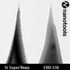
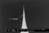
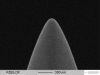
Finally, to obtain the best resolution possible, an adequate AFM probe has to be chosen. Usually, we are talking about high resolution AFM probes with an AFM tip radius below 3nm compared to a mean AFM tip radius of standard AFM probes with 7 to 10nm. Structures can only be resolved if their radius or distance is larger than the AFM tip radius. For example, a 5nm gap cannot be resolved properly with a 7nm radius AFM tip, whereas an AFM tip with a radius of 3nm can correctly image this structure.
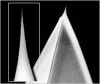
There are two approaches to manufacture high-resolution AFM tips: The first approach is to further refine the AFM tip apex of a silicon AFM tip. A complex refining process, the so-called AFM tip sharpening is applied at the end of the standard AFM probes manufacturing process to finally obtain AFM tip radii around and below 3nm. The second method is to grow an extra AFM tip made from high density carbon at the apex of the silicon AFM tip pyramid. Carbon gases are introduced into a vacuum where the AFM tip is located. A well-defined electron beam locally activates the surfaces and carbon atoms will agglomerate. By this method simple geometries of diamond-like-carbon can be generated. Usually, thin cylinders or needles with outstanding characteristics in terms of hardness are created. Those carbon extra-AFM tips can be manufactured with AFM tip apex radii down to 1nm.
Sort by:
29 results


BudgetComboBox
Mixed Box with 50 BudgetSensors AFM probes of your choice
Coating:
various
Tip Shape: various
Tip Shape: various

SuperSharp Enhanced
Ultrasharp EBD AFM whisker for high-resolution, non-contact AFM
Coating:
Reflective Aluminum
Tip Shape: Cone Shaped,Supersharp,EBD
Tip Shape: Cone Shaped,Supersharp,EBD
AFM Cantilever:
F
320 kHz
C
40 N/m
L
120 µm
SuperSharpStandard-NCH
SuperSharp diamond-like EBD whisker for non-contact AFM
Coating:
Reflective Aluminum
Tip Shape: Cone Shaped,Supersharp,EBD
Tip Shape: Cone Shaped,Supersharp,EBD
AFM Cantilever:
F
330 kHz
C
40 N/m
L
125 µm
SuperSharp Enhanced-soft
Ultrasharp EBD AFM whisker for high-resolution, soft tapping AFM
Coating:
Reflective Aluminum
Tip Shape: Cone Shaped,Supersharp,EBD
Tip Shape: Cone Shaped,Supersharp,EBD
AFM Cantilever:
F
75 kHz
C
2.8 N/m
L
225 µm
SuperSharpStandard-FM
SuperSharp diamond-like EBD AFM whisker for soft tapping AFM
Coating:
Reflective Aluminum
Tip Shape: Cone Shaped,Supersharp,EBD
Tip Shape: Cone Shaped,Supersharp,EBD
AFM Cantilever:
F
75 kHz
C
2.8 N/m
L
225 µm

SSS-SEIHR
SuperSharp, Special Tapping Mode AFM Probe
Coating:
Reflective Aluminum
Tip Shape: Supersharp
Tip Shape: Supersharp
AFM Cantilever:
F
130 kHz
C
15 N/m
L
225 µm
SSS-SEIH
SuperSharp, Special Tapping Mode AFM Probe
Coating:
none
Tip Shape: Supersharp
Tip Shape: Supersharp
AFM Cantilever:
F
130 kHz
C
15 N/m
L
225 µm

NW-SSS-SEIH
SuperSharp, Special Tapping Mode AFM Probe
Coating:
none
Tip Shape: Supersharp
Tip Shape: Supersharp
AFM Cantilever:
F
130 kHz
C
15 N/m
L
225 µm
NANOSENSORS™ Special Developments List (SDL)
Special AFM Probes etc. Showcasing NANOSENSORS™ Expertise
Coating:
various
Tip Shape: various
Tip Shape: various