Conductive AFM Probes
Originally, the first scanning probe technique developed was dealing with conductive probes: Scanning Tunneling Microscopy (STM), a technique where a sharped Tungsten wire tip was scanned across a surface, whilst controlling the tunneling current between STM tip and surface. Honored with the Physics Nobel Prize in 1986, the major drawback was, that Scanning Tunneling Microscopy was limited to conductive surfaces only.
To expand the main STM sample information – topography – from conductive to arbitrary surfaces, Scanning- or Atomic Force Microscopy (AFM) was developed. A bunch of characterization methods were developed for AFM and also the electrical properties of surfaces came into focus.
As the standard AFM probes materials are not conductive (they are either insulating or quickly forming an insulating surface oxide layer), AFM tips and AFM cantilevers have to be coated with a conductive material to allow a current flow.
In the short history of Atomic Force Microscopy almost every metal or alloy available in semiconductor and MEMS manufacturing technology was already applied to AFM probes. Metals provide excellent conductivity are easy to process and relatively inexpensive. However, only a few materials prevailed and continue to be used for standard electrically conductive AFM probes: cobalt-chromium initially intended for Magnetic Force Microscopy is used as a conductive layer as well as platinum, a noble metal without the drawback of forming an – eventually insulating – metal oxide. To increase the hardness of platinum layers a small amount of (harder) Iridium is added. Therefore, usually, all platinum coated AFM probes consist of 95% platinum with a 5% iridium portion, often denoted as PtIr. Gold is commonly used for improving the suitability of AFM cantilevers for functionalization, attaching biological material to the AFM tip. Like platinum, gold is a noble metal that doesn´t form oxides, but it is remarkably softer than platinum and rubs off the AFM tip more easily than platinum. In general, all metallic coatings are not suitable for being used in contact mode AFM for a longer period of time because of the AFM tip wear effect. Metallic coatings should be normally used for Lift Mode AFM techniques like Electrostatic Force Microscopy or Kelvin Probe Force Microscopy.
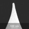
To overcome the wear-out problem of the relatively soft metal coatings many other, more resistant coatings are being used: coating an AFM probe with an extremely hard diamond coating requires a certain thickness, which results in AFM tip radii commonly in the 100 nm regime. Also, the conductivity of diamond is about 10 times smaller compared to metal. A compromise in terms of conductivity, hardness and resolution are platinum silicide AFM probes.
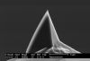
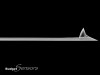
Diamond coating 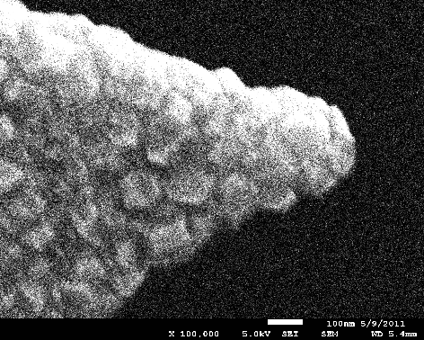
Diamond, the hardest material in the world, an extremely long-lasting coating.
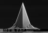
Platinum iridium coating 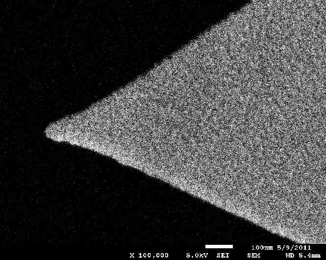
Small radius, excellent conductivity.
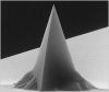
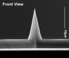
Platinum silicide AFM tip 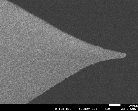
Small radius, excellent conductivity, good wear-out behavior.
AFM applications using a conductive AFM probe mainly split up into two fields: Firstly, methods where the AFM probe is in contact with the surface and an electrical current occurs. And secondly, the electrostatic or lift mode techniques.
Conductive AFM (c-AFM) is performed in contact mode. Basically, the conductively coated AFM probe is in contact with the sample surface and a bias voltage is applied between AFM tip and sample. The measured current gives information about the electrical properties of the scanned area. Depending on the method, well defined forces are applied to the AFM tip. Therefore, the conductive coating used for those applications has to show a good resistance against wear
Scanning Capacitance Microscopy (SCM) is used to map the carrier concentrations in semiconductor samples. The principle is, that a Metal-Oxide-Semiconductor (MOS) capacitor structure is formed, where the conductive AFM tip acts as the “metal” part of the capacitor. By applying an overlaying DC and AC voltage, type and quantity of dopant atoms could be analyzed. Normally, an AFM cantilever with a medium stiffness is used here, stiff enough to ensure a stable contact which guarantees a consistent capacitor area. Wear resistant coatings like Diamond or Platinum Silicide are used for SCM applications on any type of AFM cantilever. We recommend CDT-CONTR or PtSi-CONT, CDT-FMR or PtSi-FM, CDT-NCHR or PtSi-NCH as well as All-In-One-DD AFM probes for Scanning Capacitance Microscopy.
Conductive AFM (c-AFM), Tunneling AFM (TUNA), I-V-Spectroscopy: Simply by applying a bias voltage to an AFM tip or sample the local conductivity or its variations could be observed. The principle of c-AFM and TUNA is identical, c-AFM is the more general description whereas TUNA normally is related to the characterization of insulating layers. In c-AFM usually only a few orders of magnitudes in current are observed, whereas the range of TUNA currents can vary from extremely low tunneling- up to high breakdown currents of insulating layers. Additionally, the characterization of insulating layers could be performed in different ways. Either by applying a constant bias voltage or by ramping the voltage at a fixed place of the scan. This technique is called I-V-Spectroscopy. Again, wear resistant coatings like doped Diamond or Platinum Silicide on various AFM cantilever types, depending on the application, are the choice for c-AFM and TUNA applications.
Scanning Spreading Resistance (SSRM): the second method to obtain information on semiconductor dopants and the position of p-n-junctions is SSRM. In its macroscopic version, 2 needles with defined radii and spacing are pressed through the native oxide into the semiconductor. A defined voltage is applied and the current is being measured. Usually, the surface is beveled in a very shallow angle and therefore, one obtains a high spatial resolution. In SSRM, due to the small radius of an AFM tip no sample preparation (beveling) is needed. Scanning Spreading Resistance is performed on cross-section of samples. To penetrate the native oxide an AFM cantilever with a very high force constant is needed. Only Diamond as a conductive coating is able to withstand the high forces of SSRM. Usually CDT-NCHR, DDESP or All-In-One-DD are used for SSRM.
Contrary to c-AFM applications performed in contact with the sample, the so-called Lift Mode techniques are applications where in a first line scan the topography is recorded, and during the retrace in a well-defined height above the sample, the interaction of the electrically charged AFM probe with the charges on the sample are recorded. For these applications medium hard AFM cantilevers are used: stiff enough to ensure a proper AC or Tapping Mode topography imaging and soft enough to detect the changes in the electrical field between AFM tip and sample. As the wear in these modi is low, thin coatings with highly conductive materials as Platinum or Platinum Silicides are used here.
In Electrostatical Force Microscopy (EFM). After imaging the topography in AC or Tapping Mode AFM during one direction of the scan, the AFM tip is lifted up and traced back with a defined height above the surface. Charges on the biased conductively coated AFM probe are interacting via electrostatic forces with charges on the sample. If the charge distribution changes the electric force gradient changes and the AFM cantilever is bent which is detected by the laser deflection.
Kelvin Probe Force Microscopy (KPFM). KPFM works analog to EFM. Additionally, in the lifted scan trace an AC voltage is applied to the AFM tip, generating a capacitive force. Compensating this capacitive force by adding and mapping another DC voltage gives information about the work function of the investigated materials.
For all Lift Mode techniques, Electrostatical Force Microscopy as well as Kelvin Probe Force Microscopy, AFM probes coated with a low resistivity material like Platinum or Platinum Silicide on a medium hard soft tapping or force modulation AFM cantilever are recommended (PtSi-FM, PPP-EFM, EFM, ElectriMulti75-G).
Sort by:
82 results


BudgetComboBox
Mixed Box with 50 BudgetSensors AFM probes of your choice
Coating:
various
Tip Shape: various
Tip Shape: various
Tap150E-G
Electrical, Soft Tapping Mode AFM Probe
Coating:
Electrically Conductive
Tip Shape: Rotated
Tip Shape: Rotated
AFM Cantilever:
F
150 kHz
C
5 N/m
L
125 µm

PPP-CONTPt
Electrical, Contact Mode AFM Probe
Coating:
Electrically Conductive
Tip Shape: Standard
Tip Shape: Standard
AFM Cantilever:
F
13 kHz
C
0.2 N/m
L
450 µm
PPP-CONTSCPt
Electrical, Contact Mode AFM Probe with Short AFM Cantilever
Coating:
Electrically Conductive
Tip Shape: Standard
Tip Shape: Standard
AFM Cantilever:
F
25 kHz
C
0.2 N/m
L
225 µm

ATEC-CONTPt
Electrical, Contact Mode AFM Probe with REAL Tip Visibility
Coating:
Electrically Conductive
Tip Shape: Visible
Tip Shape: Visible
AFM Cantilever:
F
15 kHz
C
0.2 N/m
L
450 µm

ARROW-CONTPt
Electrical, Contact Mode AFM Probe with Tip at the Very End of the Cantilever
Coating:
Electrically Conductive
Tip Shape: Arrow
Tip Shape: Arrow
AFM Cantilever:
F
14 kHz
C
0.2 N/m
L
450 µm
CONTPt
Electrical, Contact Mode AFM Probe
Coating:
Electrically Conductive
Tip Shape: Standard
Tip Shape: Standard
AFM Cantilever:
F
13 kHz
C
0.2 N/m
L
450 µm
ContE-G
Electrical, Contact Mode AFM Probe
Coating:
Electrically Conductive
Tip Shape: Rotated
Tip Shape: Rotated
AFM Cantilever:
F
13 kHz
C
0.2 N/m
L
450 µm

HQ:CSC37/Pt
AFM Probe with 3 Different Electrical, Contact Mode AFM Cantilevers
Coating:
Electrically Conductive
Tip Shape: Rotated
Tip Shape: Rotated
AFM Cantilevers: 3
1
2
3
F
40 kHz
20 kHz
30 kHz
C
0.8 N/m
0.3 N/m
0.4 N/m
L
250 µm
350 µm
300 µm
SCM-PIC
Electrical, Contact Mode AFM Probe
Coating:
Electrically Conductive
Tip Shape: Standard
Tip Shape: Standard
AFM Cantilever:
F
13 kHz
C
0.2 N/m
L
450 µm
SCM-PIT
Electrical, Force Modulation AFM Probe
Coating:
Electrically Conductive
Tip Shape: Standard
Tip Shape: Standard
AFM Cantilever:
F
75 kHz
C
2.8 N/m
L
225 µm
ATEC-FMAu
Gold Coated Force Modulation AFM Probe with REAL Tip Visibility
Coating:
Gold Overall
Tip Shape: Visible
Tip Shape: Visible
AFM Cantilever:
F
85 kHz
C
2.8 N/m
L
240 µm
HQ:CSC17/Pt
Electrical, Contact Mode AFM Probe
Coating:
Electrically Conductive
Tip Shape: Rotated
Tip Shape: Rotated
AFM Cantilever:
F
13 kHz
C
0.18 N/m
L
450 µm
PPP-FMAu
Gold Coated Force Modulation AFM Probe
Coating:
Gold Overall
Tip Shape: Standard
Tip Shape: Standard
AFM Cantilever:
F
75 kHz
C
2.8 N/m
L
225 µm
PNP-TR-Au
Gold Coated Silicon Nitride AFM Probe
Coating:
Gold Overall
Tip Shape: Pyramid
Tip Shape: Pyramid
AFM Cantilevers: 2
1
2
F
67 kHz
17 kHz
C
0.32 N/m
0.08 N/m
L
100 µm
200 µm
HQ:NSC18/Cr-Au
Gold Coated Force Modulation AFM Probe
Coating:
Gold Overall
Tip Shape: Rotated
Tip Shape: Rotated
AFM Cantilever:
F
75 kHz
C
2.8 N/m
L
225 µm
HQ:NSC19/Cr-Au
Gold Coated Force Modulation AFM Probe
Coating:
Gold Overall
Tip Shape: Rotated
Tip Shape: Rotated
AFM Cantilever:
F
65 kHz
C
0.5 N/m
L
125 µm
HQ:NSC35/Cr-Au
AFM Probe with 3 Different Gold Coated Tapping Mode AFM Cantilevers
Coating:
Gold Overall
Tip Shape: Rotated
Tip Shape: Rotated
AFM Cantilevers: 3
1
2
3
F
205 kHz
300 kHz
150 kHz
C
8.9 N/m
16 N/m
5.4 N/m
L
110 µm
90 µm
130 µm
HQ:NSC36/Cr-Au
AFM Probe with 3 Different Gold Coated Force Modulation Mode AFM Cantilevers
Coating:
Gold Overall
Tip Shape: Rotated
Tip Shape: Rotated
AFM Cantilevers: 3
1
2
3
F
90 kHz
130 kHz
65 kHz
C
1 N/m
2 N/m
0.6 N/m
L
110 µm
90 µm
130 µm

3XC-GG
AFM Probe with 3 Different Gold Coated AFM Cantilevers for Various Applications and AFM Tips at the Very End of the AFM Cantilevers
Coating:
Gold Overall
Tip Shape: Optimized Positioning
Tip Shape: Optimized Positioning
AFM Cantilevers: 3
1
2
3
F
17 kHz
150 kHz
75 kHz
C
0.3 N/m
9 N/m
2.5 N/m
L
500 µm
175 µm
240 µm